![]()
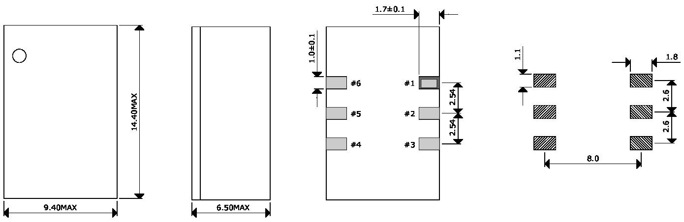
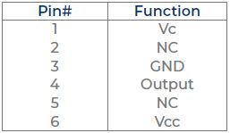
SOC14C Series – 14.4MM X 9.4MM FR4 PCB SMD 6 Pad CMOS (VC)OCXO
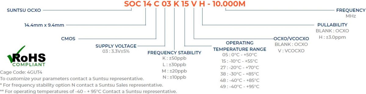
Part Numbering Guide
Electrical Parameters
| Parameters | Units | Min | Typical | Max | Remarks |
|---|---|---|---|---|---|
| Frequency Range | MHz | 10 | 40 | ||
| Frequency Tolerance at +25ºC | ppm | -0.5 | +0.5 | ||
| Freq. Stability vs. Op Temp. | ppb | -10 | +10 | See part numbering guide for options. | |
| Freq. Stability vs. Supply Voltage | ppb | -10 | +10 | VDD±5% Change | |
| Freq. Stability vs. Load | ppb | -10 | +10 | ±5% Change | |
| Freq. Stability vs. Aging/Year | ppm | -1 | +1 | ||
| Operating Temperature | °C | -40 | +95 | See part numbering guide for options. | |
| Storage Temperature | °C | -55 | +125 | ||
| Supply Voltage (VDD) | V | 3.135 | 3.3 | 3.465 | |
| Power Consumption At Turn On | W | 2.0 | |||
| Power Consumption At 25°C | W | 0.5 | |||
| Current Voltage (VC) | V | 0 | 3.3 | ||
| Control Middle Voltage | V | 1.65 | |||
| Pullability | ppm | ±3.0 | |||
| Linearity | % | 10 | |||
| VC Input Impedance | kΩ | 50 | |||
| Deviation Slope | Positive | ||||
| Output Logic (CMOS) | pF | 15 | |||
| Output Logic Level - High (VOH) | V | 0.9*VDD | |||
| Output Logic Level - Low (VOL) | V | 0.1*VDD | |||
| Rise Time (TR) And Fall Time (TF) | nS | 5 | |||
| Symmetry (Duty Cycle) | % | 45 | 50 | 55 | |
| Start-Up Time | ms | 3 | |||
| Warm-Up Time | Mins | 3 | |||
| Phase Noise (Typical) 1Hz Offset | dBc/Hz | -60 | |||
| Phase Noise (Typical) 100Hz Offset | dBc/Hz | -120 | |||
| Phase Noise (Typical) 1KHz Offset | dBc/Hz | -150 |
Outline Drawing & Recommended Landed Pattern
All dimensions are in millimeters (mm) unless otherwise noted. Drawings are not to scale.