

Key Factors that Affect Antenna Performance on a PCB
To develop elegant solutions for complex engineering challenges without being constrained by component limitations, it is essential to consider the key variables that influence RF performance and how signals move through the system.
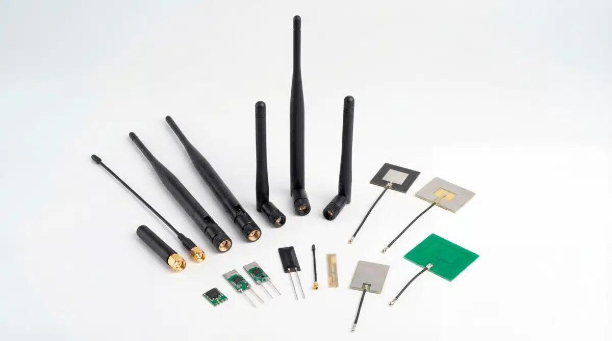
- Ground Plane Size and Clearance: For many common surface-mount antennas, like inverted-F or chip antennas, the PCB ground plane serves as the other half of the dipole. For very compact wireless designs such as access control systems and secure authentication modules, an NFC antenna is often used, where near-field coupling is highly sensitive to ground plane size, clearance, and nearby copper detuning effects. If this ground plane is too small, the antenna won’t resonate at the desired frequency. On the other hand, if copper planes are positioned too close to the antenna’s radiating element, they can couple with the RF energy and cause detuning.
- Routing of High-Speed Traces: Digital signals, including high-frequency clocks and memory buses, produce substantial electromagnetic interference (EMI). In precision RF systems, stable timing sources such as an oven controlled crystal oscillator (OCXO) are often used to minimize noise and maintain signal integrity. When high-speed traces run close to the RF front end, their harmonics increase the noise floor, reducing receiver sensitivity and significantly restricting wireless range.
- Via Placement: Vias are essential for connecting ground planes to form a stable, continuous reference. However, incorrectly placed vias—particularly via stubs on the RF feedline—can function as small antennas, leading to impedance mismatches and signal reflections.
- The Physical Device Enclosure: Your layout cannot be isolated, as the plastic or metal enclosure around the PCB significantly influences performance. Plastics, with a dielectric constant higher than air, slow electromagnetic waves and decrease the antenna’s resonant frequency. Metal enclosures can entirely block radiation, necessitating external antennas or precisely engineered slots.
Common Antenna Placement Mistakes
Even experienced engineers can make subtle layout errors. Steering clear of these common issues will save you from frustration and time spent searching for non-standard parts or undergoing costly, lengthy re-qualification processes.
Most embedded antennas are designed to radiate outward from the edge or corner of a PCB. Placing an antenna in the center surrounds it with substrate and copper, trapping the RF energy and drastically reducing efficiency.
Antenna manufacturers specify strict keepout zones in their datasheets. A common mistake is clearing the copper on the top layer but neglecting to remove ground planes, power planes, and traces on the inner and bottom layers directly underneath the antenna.
Placing an antenna close to switching power supplies, motor drives, or microcontrollers results in reduced receiver sensitivity.
Relying on a 50-ohm trace to perfectly match a chip antenna without a tuning circuit is risky. Skipping the pads for a Pi matching network – which includes a series component and two shunt components – leaves you without a way to tune the antenna after the board is made.
Best Practices for Antenna Placement in Wireless Devices
To ensure strong performance and make your design process easier, follow these best practices for antenna placement on PCB design:
Utilize Edges and Corners
Always place your antenna at the edge of the PCB, ideally in a corner. This allows the antenna to have the maximum clearance to radiate freely into space in at least three directions. Choosing to locate your antenna at the edges and corners improves signal view and reach, helping devices better receive signals over longer distances, especially in complex indoor environments.
Enforce 3D Keepout Zones
Consider the keepout area as a three-dimensional cylinder that extends through all PCB layers. No copper, traces, or components are allowed within this zone on any layer.
Stitch the Ground Plane
Place a dense array of stitching vias along the RF ground plane’s edge to stop edge-emitting radiation and maintain a solid, continuous ground reference for the RF transceiver.
Isolate the RF Section
Physically isolate the analog/RF section of your board from the digital and power sections. If needed, add a shielding can over the transceiver IC to block EMI from radiating into or out of the RF circuitry.
Design for 50-Ohm Impedance
Use co-planar waveguide (CPW) or microstrip calculations to verify that the trace connecting the transceiver to the antenna is precisely 50 ohms. Keep this trace as short and straight as physically possible.
If standard components do not satisfy your rigorous design needs, working with experienced electronics parts suppliers, like Suntsu’s engineers, can assist you in developing custom components that are specifically designed to fit your board’s unique footprint and spatial constraints.
Reduce RF Design Risk with Expert Antenna Placement
Mastering antenna placement in PCB design requires a comprehensive understanding of electromagnetics, precise layout execution, and thorough real-world testing. By respecting keepout zones, utilizing edge placement, isolating noisy components, and preparing for impedance matching, you can achieve dependable wireless performance and ensure your product launches on time.
However, you don’t have to handle complex RF challenges on your own. Sometimes, all you need is to talk to another engineer about a custom solution or a difficult design problem. Suntsu is committed to being that dependable partner. Whether you require expert help through our Engineering Design Services to plan your RF front end, comprehensive support from our Engineering Services division, or reliable execution with our Full Turnkey and Partial Turnkey PCB Assemblies, we are ready to assist you in turning your most ambitious designs into reality.
Minimize the risk of costly board respins and keep your project on schedule by securing the exact components your RF design requires. Request a quote today to partner with our experts and find elegant solutions to your most complex engineering problems.
FAQs
Placing an internal surface-mount antenna inside a fully enclosed metal chassis is a recipe for a Faraday cage – your signal will not escape. If you musts use a metal enclosure, you have three primary options:
- Use an external antenna: Route your RF signal to a panel-mount SMA or U.FL connector.
- Design a hybrid enclosure: Create an “RF window” by using an RF-transparent plastic or fiberglass cap directly over the antenna’s location.
- Utilize a slot antenna: You can engineer the metal enclosure itself to act as the antenna by cutting a precisely tuned slot into the metal and exciting it with a microstrip feed, through this requires complex 3D electromagnetic simulation.
Yes. The substrate’s dielectric constant (Dk) directly affects the velocity of propagation and, consequently, the effective wavelength of your RF signal. Standard RF4 has a relatively high and variable Dk (around 4.2 to 4.8), which can shift the resonant frequency of your antenna from batch to batch. High-frequency laminates like Rogers have a lower, tightly controlled Dk and a lower loss tangent (Df). If you switch substrates, you must recalculate your 50-ohm trace widths (CPW or microstrip) and re-verify the manufacturer’s keepout zone recommendations, as the fringing fields will behave differently.
Absolutely not. Batteries are encased in metal, and LCD/OLED displays have large metallic backplanes and generate significant digital noise. If placed within the radiation pattern or keepout zone of your antenna, these components act as parasitic elements. They will violently detune the antenna, absorb RF energy, and reflect signals back into your transceiver. Treat batteries and displays as solid ground planes and enforce a strict 3D keepout distance.
For an unbalanced antenna (like a monopole or inverted-F chip antenna), the PCB ground plane acts as the counterpoise – effectively the other half of the antenna. As a rule of thumb, the ground plane extending away from the antenna should be at least a quarter-wavelength (λ/4) of your lowest operating frequency. For example, at 2.4GHz, you need a minimum of roughly 31mm of continuous ground plane. If your board is smaller than this, the antenna’s efficiency will plummet, and its resonant frequency will shift dramatically.
Antenna placement must be the very first step in your layout process. RF constraints are non-negotiable. Place the antenna at the optimal edge or corner first, then place your RF transceiver as close as possible to minimize feedline loss. Only after the RF front-end is locked in should you route your power supplies, microcontrollers, and high-speed digital buses, ensuring they are kept far away from the RF section.
Related Content