![]()
SST75C Series – 7.0MM X 5.0MM Ceramic Stratum 3 SMD 10 Pad CMOS (VC)TCXO
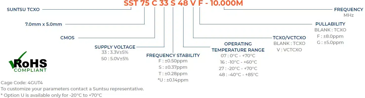
Part Numbering Guide
Electrical Parameters
| Parameters | Units | Min | Typical | Max | Remarks |
|---|---|---|---|---|---|
| Frequency Range | MHz | 5 | 26 | ||
| Frequency Tolerance at +25ºC | ppm | -4.6 | +4.6 | ||
| Freq. Stability vs. Op Temp. | ppm | -0.28 | +0.28 | See part numbering guide for options. | |
| Freq. Stability vs. Supply Voltage | ppm | -3.7 | +3.7 | ||
| Operating Temperature | °C | -40 | +85 | See part numbering guide for options. | |
| Storage Temperature | °C | -55 | +125 | ||
| Supply Voltage (VDD) - 3.3V Option | V | 3.135 | 3.3 | 3.465 | |
| Supply Voltage (VDD) - 5.0V Option | V | 4.750 | 5.0 | 5.250 | |
| Current (IDD) | mA | 6 | |||
| Current Voltage (VC, VCTCXO) - 3.3V Option | V | 0.5 | 2.5 | ||
| Current Voltage (VC, VCTCXO) 5.0V Option | V | 0.5 | 2.5 | ||
| Pullability (VCTCXO) | ppm | ±5.0 | ±8.0 | See part numbering guide for options. | |
| Linearity (VCTCXO) | % | 10 | |||
| Output Load (CMOS) | pF | 15 | |||
| Output Logic Levels High (VOH) | V | 0.9*VDD | |||
| Output Logic Levels Low (VOL) | V | 0.1*VDD | |||
| Rise (TR) and Fall (TF) Time | ns | 5 | |||
| Symmetry (Duty Cycle) | % | 45 | 50 | 55 | |
| Tri-State Input Voltage (Enabled) | V | 0.7*VDD | |||
| Tri-State Input Voltage (Disabled) | V | 0.3*VDD | |||
| Start-Up Time | ms | 10 | |||
| VC Input Impedance (VCTCXO) | kΩ | 100 | |||
| Phase Noise (Typical) 100Hz Offset | dBc/Hz | -120 | |||
| Phase Noise (Typical) 1KHz Offset | dBc/Hz | -140 | |||
| Phase Noise (Typical) 10KHz Offset | dBc/Hz | -148 |
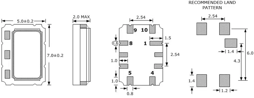
Outline Drawing & Recommended Landed Pattern
All dimensions are in millimeters (mm) unless otherwise noted. Drawings are not to scale.