![]()
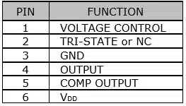
SVC75L Series – 7.0MM X 5.0MM Ceramic SMD 6 Pad LVDS VCXO
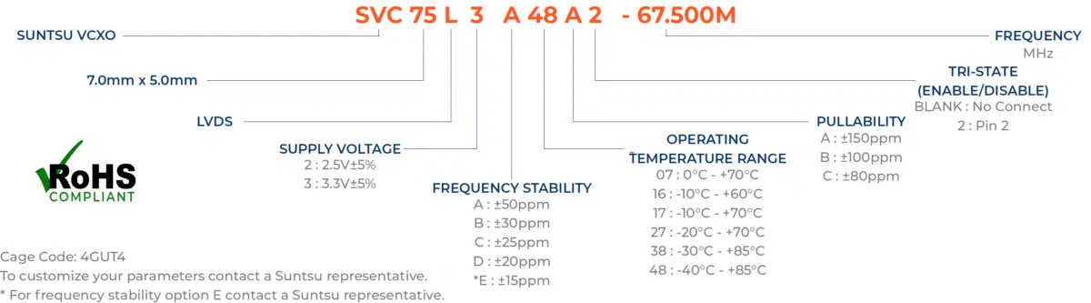
Part Numbering Guide
Electrical Parameters
| Parameters | Units | Min | Typical | Max | Remarks |
|---|---|---|---|---|---|
| Frequency Range | MHz | 9.5 | 80 | ||
| Frequency Stability (Includes Initial Tolerance at 25°C, Frequency Stability over Operating Temperature, Output Load Change, Supply Voltage Change, and First Year Aging at 25°C.) | ppm | -20 | +20 | See part numbering guide for options. | |
| Operating Temperature | °C | -40 | +85 | See part numbering guide for options. | |
| Storage Temperature | °C | -55 | +125 | ||
| Supply Voltage (VDD) - 2.5V Option | V | 2.375 | 2.5 | 2.625 | Only available with AT-Cut Fundamental. |
| Supply Voltage (VDD) - 3.3V Option | V | 3.135 | 3.3 | 3.465 | Available with AT-Cut Fundamental and PLL. |
| Current (IDD) - 2.5V Option | mA | 50 | |||
| Current (IDD) - 3.3V Option | mA | 60 | |||
| Current Voltage (VC) 2.5V Option | V | 0.2 | 2.3 | ||
| Current Voltage (VC) 3.3V Option | V | 0.3 | 3.0 | ||
| Pullability | ppm | ±50 | ±100 | ±150 | See part numbering guide for options. |
| Linearity | % | 10 | |||
| Output Load (LVDS) | Ω | 100 | |||
| Output Logic Levels High (VOH) | V | 1.43 | 1.6 | ||
| Output Logic Levels Low (VOL) | V | 0.9 | 1.1 | ||
| Rise (TR) and Fall (TF) Time | ns | 0.4 | 0.8 | ||
| Symmetry (Duty Cycle) | % | 45 | 50 | 55 | |
| Output Logic Levels High (VOH) | V | 0.7*VDD | |||
| Output Logic Levels Low (VOL) | V | 0.3*VDD | |||
| Start-Up Time | ms | 10 | |||
| Phase Jitter (12kHz ~ 20MHz) | ps | 0.4 | 1 | AT-CUT Fundamental | |
| Phase Jitter (12kHz ~ 20MHz) | ps | 3 | 5 | PLL (Phase Lock Loop) |
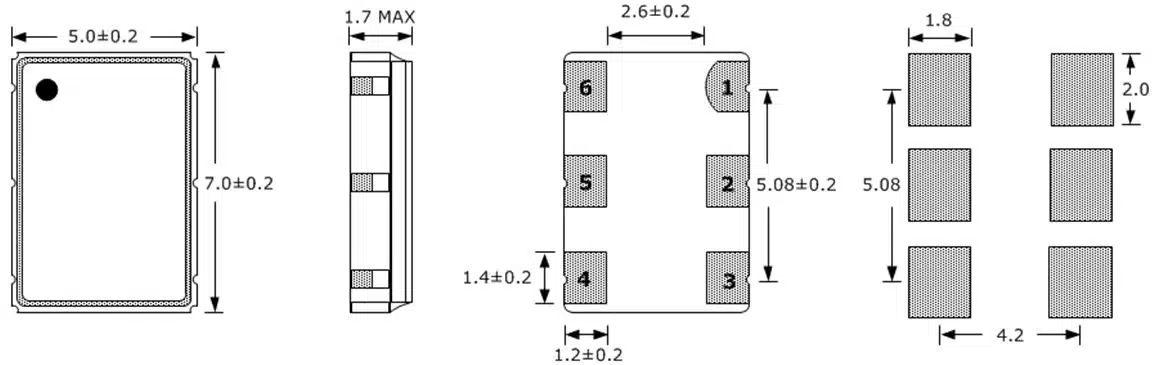
Outline Drawing & Recommended Landed Pattern
All dimensions are in millimeters (mm) unless otherwise noted. Drawings are not to scale.