

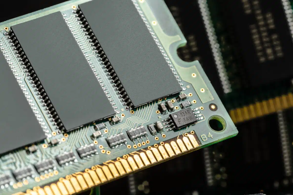
Predicting RAM Capacity Requirements for Modern Inference Models
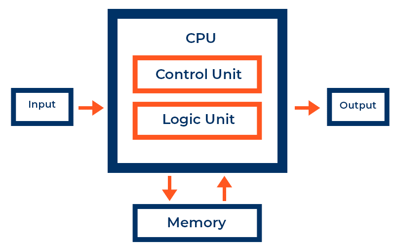
One of the most common questions during the schematic phase is: how much memory does edge AI need? The answer is never a fixed number; it depends on model parameters, bit precision, and active workspace buffers.
- Model Parameter Storage: A model with 10 million parameters using 16-bit (FP16) precision will require 20MB just for the static weights.
- Quantization Impact: By utilizing 8-bit integer (INT8) or even 4-bit quantization, engineers can reduce the memory footprint by 50% to 75%. This is essential for fitting complex models into the internal SRAM of a microcontroller.
- Activation Buffers: During inference, the system must store intermediate results (activations) for each layer. For high-resolution computer vision models, these activations can often exceed the size of the model itself.
- Inference Engine Overhead: Modern runtimes like TensorFlow Lite or ONNX require a workspace memory (heap) to manage tensors during execution.
Even with aggressive optimization, advanced edge vision models usually require between 4GB and 16GB of external DRAM. Underestimating this need can cause severe out-of-memory (OOM) errors during inference, while overestimating raises both the BOM cost and standby power consumption. For detailed guidance on choosing the right components, see our technical blog: Memory IC essentials: selecting the right components for your project.
Evaluating LPDDR4x and LPDDR5 Efficiency for Power-Sensitive Designs
Choosing between LPDDR4x and LPDDR5 is a key technical decision for high-performance edge devices. While both provide low-power features, they differ markedly in architecture, affecting efficiency and maximum throughput.
| Feature | LPDDR4x | LPDDR5 |
|---|---|---|
| Max Data Rate | 4266 MT/s | 6400 MT/s |
| I/O Voltage (VDDQ) | 0.6V | 0.5V (VDD2H) |
| Architecture | Single-ended clock | Differential clock / WCK |
| Power Efficiency | Standard LP Features | Dynamic Voltage Scaling / Deep Sleep |
LPDDR4x is the dominant memory solution in medical and industrial sectors, providing proven reliability and lower supply risk. It features a reduced I/O voltage to conserve power during fast data transfers.
LPDDR5 features like “Data-Copy” and “Write-X” help minimize internal data transfer, while an enhanced sleep mode is crucial for battery-powered devices carrying out periodic inference. Jeju Semiconductor (JSC), an authorized partner of Suntsu, focuses on developing these low-power Integrated Circuits and memory modules. Their significance in the market is further detailed in Tiny Chips, Big Impact: The Rise of JSC in the Memory Semiconductor Sector.
Choosing Local AI Storage: eMMC vs UFS
Non-volatile storage permanently holds the AI model weights. The process of retrieving these weights into RAM during a “cold start” or model swap can become a major bottleneck.
- eMMC (embedded Multi-Media Controller): eMMC 5.1 uses a parallel, half-duplex interface, allowing only read or write operations at a time. With a maximum speed of about 400 MB/s, it suits smaller models where fast boot times are not essential. When specifying highly reliable eMMC solutions, Suntsu’s Engineering Services team frequently qualifies high-grade NAND flash from authorized partners like ESMT and Jeju Semiconductor (JSC).
- UFS (Universal Flash Storage): UFS employs a serial, full-duplex interface modeled after SCSI architecture, enabling concurrent read and write operations with speeds surpassing 1,200 MB/s. To meet these high-speed, demanding UFS requirements, Suntsu partners with Flexxon to deliver storage that guarantees industrial-grade longevity and rapid data transfer.
For applications requiring real-time model switching, like a smart camera switching from object detection to facial recognition based on a trigger, UFS is the best option. It minimizes the “blind time” during transitions.
Deploying NOR Flash for Deterministic Latency and XiP Capabilities
Although NAND flash (eMMC/UFS) is favored for high-density storage, NOR flash continues to be essential for certain Edge AI applications because of its distinct architectural benefits.
The main benefit of NOR flash is its Execute-in-Place (XiP) feature. Unlike NAND flash, which needs code to be copied to RAM before running, NOR enables the processor to run instructions directly from the flash memory. This is essential for ultra-low latency applications where every millisecond of boot-up or response time matters.
In safety-critical industrial applications, NOR flash offers much greater reliability and quicker random read access. Suntsu collaborates with ESMT to deliver industrial-grade memory solutions built to endure tough environments while ensuring data integrity. For a comprehensive comparison of these technologies, see the NOR Flash Guide 2026: Architecture, Reliability, and NAND vs NOR.
Mitigating Engineering Risks and Enhancing BOM Stability
Even a technically excellent design can fail if the selected components are difficult to source. Hardware engineers often encounter ‘Design Restrictions’ when a standard part doesn’t match the specific footprint or power needs of their project. This issue is often worsened by the ‘One Missing Part’ problem, where a $250,000 assembly process is halted because of a single missing memory IC. These challenge often extend beyond memory and storage components to include sourcing constraints on discrete semiconductors, which support power management, switching, and signal control across embedded and IoT systems.
Suntsu’s hybrid model provides a pathway out of these engineering roadblocks:
![]()
Design Alternatives: If a specified memory module goes End-of-Life (EOL), our engineering team identifies drop-in replacements that meet or exceed the original specs
![]()
Custom Components: When off-the-shelf parts won’t fit the envelope, we can assist in creating Custom Components tailored to the design.
![]()
Reliability Verification: Our thorough Quality Assurance Process guarantees that all sourced parts—whether from franchised lines or independent suppliers—adhere to the technical standards essential for high-reliability organizations.
By incorporating Shortage Mitigation and Global Sourcing capabilities early in the design process, engineers can facilitate a smooth transition from prototype to production, avoiding the typical 52-week delays common in the AI infrastructure era.

Secure the high-performance memory components your Edge AI design demands while eliminating the risk of long lead times and supply chain disruptions. Partner with Suntsu Electronics today to build a resilient BOM and keep your production schedule on track.
FAQs
The jump to LPDDR5 involves significantly higher data rates (up to 6400 MT/s), which necessitates much tighter control over signal integrity. Designers must account for more stringent length-matching, impedance control, and the transition to a differential clock (WCK) architecture. Suntsu’s Board Characterization Services can help your team simulate these high-speed buses to prevent data corruption before you commit to a mass production run.
Yes. Standard commercial memory is typically rated for 0°C to 70°C, which is often insufficient for industrial enclosures. For these applications, you should specify “Industrial Temperature” (-40°C to 85°C) or “Automotive Grade” (-40°C to 105°C or higher) components. Suntsu’s Engineering Services team can assist in identifying the correct temperature-grade versions of parts to ensure reliability in harsh conditions.
Swapping large model weights into RAM involves high-volume read/write cycles. While read operations are less taxing, the constant “wear” on NAND cells can lead to premature failure. To mitigate this, look for storage with advanced wear-leveling algorithms and high “Total Bytes Written” (TBW) ratings.
Data corruption, or “bit-rot,” can occur over time in flash memory, leading to a loss of model accuracy or system crashes. To prevent this, engineers should specify memory with robust ECC (Error Correction Code) and “Data Refresh” features that periodically scan and relocate data to healthy cells. This is especially vital for high reliability organizations where system failure is not an option.
While SD cards are convenient for development, they often lack the vibration resistance and thermal stability required for professional full box builds. For production, we recommend soldered-down solutions like eMMC or UFS, or industrial-grade mSATA/M.2 modules that offer superior shock resistance and more reliable electrical connections.
Related Content