
Architecture & The Physical Reality: NAND vs. NOR Flash
The core difference in the nand vs nor flash debate is their physical memory cell layout. To most, both are non-volatile storage, but for engineers, they are as distinct as a fast highway and a busy shipping port.
Cell Structure and Connectivity
In NOR Flash, cells are linked in parallel to the bitlines, enabling independent access to each memory cell. In contrast, NAND Flash cells are connected in series, which greatly boosts density but necessitates reading data in “pages” or “blocks.”
Random Access vs. Page Access
The parallel structure of NOR Flash allows for Random Access, enabling an MCU or SoC to directly access any memory location, similar to RAM. This provides extremely low latency for read operations. On the other hand, NAND is a sequential access device; reading a single byte requires reading an entire page, typically 2KB to 16KB, which makes it less ideal for fine-grained code execution.
The Gold Standard for Execute in Place (XiP)
NOR Flash supports random access at speeds similar to some SRAMs, making it the industry standard for Execute in Place (XiP). XiP enables the processor to run code directly from the Flash chip without copying it to volatile RAM first. This minimizes the need for large, costly external DRAM and improves boot times, which is essential for automotive clusters, medical monitors, and industrial controllers that require “instant-on” functionality.
Although our SSD Deep Dive frequently highlights advancements, it is crucial to remember that SSDs (NAND-based) excel in capacity, whereas NOR flash is superior in immediacy and reliability for the kernel.
Strategic Selection: When to Choose NOR Over NAND
Choosing the appropriate memory technology involves more than just considering cost per gigabit; it also depends on the particular needs of the application’s operating environment.

If your application demands a high level of "boot-up certainty," NOR Flash is the best option. Its natural absence of bad blocks at lower densities and its high initial reliability make it a safer choice for BIOS, bootloaders, and essential firmware. Although NAND Flash prices have surged, impacting high-capacity storage markets, NOR Flash remains a stable and reliable choice for code-intensive designs.
In the medical and industrial fields, "good enough" is never sufficient. Systems like patient monitors or factory automation controllers need memory that can endure thermal cycling and preserve data accuracy over decades. NOR Flash is much less susceptible to bit-flips compared to NAND, and generally does not need the complex Error Correction Code (ECC) engines that increase overhead in NAND-based systems.
Typically, if your storage needs are under 512MB, NOR Flash is the most efficient option. For larger storage needs such as operating systems like Linux or Android, or extensive data logging, NAND Flash is preferred. However, for compact, RTOS-based systems common in modern Integrated Circuits, NOR Flash remains the primary architecture.
Interface Analysis: Serial (SPI) vs. Parallel NOR
After deciding to use NOR, the following challenge is selecting the physical interface. This decision directly affects your PCB space and your system’s throughput.
Serial (SPI) NOR Flash
- The Modern Standard: SPI NOR, including Dual and Quad-SPI (QSPI), has become the dominant interface.
- Efficiency: By using a 4-pin or 8-pin interface, it dramatically reduces the footprint on the PCB. Modern QSPI and Octal-SPI interfaces have closed the performance gap, offering throughputs that satisfy most XiP requirements.
- Design Advantage: Smaller packages (like WSON or SOIC) allow for denser board layouts, which is a key focus of our Engineering Services team when helping clients shrink their hardware footprint.
Parallel NOR Flash
- The Powerhouse: Parallel NOR uses a traditional address and data bus (e.g., 8-bit or 16-bit).
- Performance: It offers the highest possible read throughput and the lowest latency, making it ideal for high-performance legacy systems or extremely fast boot requirements.
- The Trade-off: High pin count. A 16-bit parallel interface can easily consume 40+ pins on your controller, complicating BOM Analysis and Cost Reduction efforts due to the need for larger packages and more complex PCB routing.


Engineering for Resilience
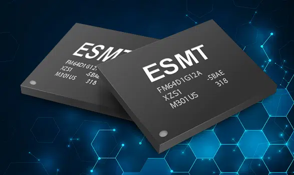
The 2026 market demands more than just a functional circuit; it demands a resilient one. Choosing NOR Flash is a strategic decision that prioritizes system integrity and boot-up reliability over raw storage volume. By understanding the architectural differences between NOR and NAND, selecting the optimal interface for your PCB, and partnering with stable suppliers like ESMT, you set your project up for long-term success.
At Suntsu Electronics, we go beyond merely shipping parts. Our Engineering Services team is prepared to support you with a range of services, including circuit board analysis and helping identify design alternatives for elusive components.
Let our experts help you mitigate sourcing risks and optimize your memory architecture for long-term reliability.
FAQs
While NOR Flash has slower program/erase times compared to NAND, it allows for granular byte-level or word-level modifications on certain architectures. For industrial and medical equipment, firmware updates are relatively infrequent compared to data logging, so the reliability of the 100k endurance cycles far outweighs the slightly longer write-on-site time.
Generally, no. Because of its physical cell structure, NOR is inherently more stable and less prone to bit-flips. While some ultra-high-density NOR (above 1Gb) or automotive-grade parts now include internal ECC, most standard designs do not require the controller-level ECC management that is mandatory for NAND.
Block locking allows engineers to write-protect specific sectors of the NOR Flash. This is essential for protecting the bootloader and core kernel from accidental corruption or malicious overwriting during field firmware updates, ensuring the device remains recoverable even if a “flash gone wrong” scenario occurs.
Uniform Sector NOR Flash has identical erase-block sizes throughout the chip (e.g., all 64KB). Boot Block architecture features a few smaller sectors (e.g., 4KB or 8KB) at the top or bottom of the memory map. These smaller blocks are optimized to store parameter data or small bootloaders without wasting the space of a full 64KB block.
While possible, it is not recommended for high-frequency logs due to the 100k P/E cycle limit. If you must use NOR, you should implement a “wear-leveling” algorithm in your firmware to distribute writes across the entire memory array, preventing specific sectors from failing prematurely.
Related Content