

What is Multi-Chip Package (MCP) Memory?
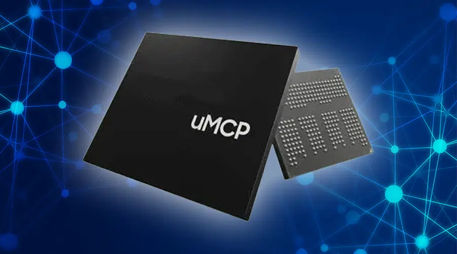
Multi-Chip Package Memory (MCP Memory) is an advanced semiconductor packaging method that integrates two or more different IC dies into a single package [1]. In memory applications, MCP usually stacks non-volatile memory like NAND Flash, which retains data without power, alongside volatile memory like DRAM, used for high-speed processing, all within a compact surface-mount form factor.
Rather than mounting separate Flash and RAM chips next to each other on a PCB, MCP Memory stacks them vertically or lines them up side-by-side within a single protective casing. They connect internally through microscopic wire bonds or advanced flip-chip techniques. This creates a single component that provides the functions of multiple independent chips, working together seamlessly to meet the system’s processing requirements.
Why MCP Memory is Critical in Modern Electronics
Adopting MCP Memory isn’t merely a technical trend; it’s a strategic necessity influenced by modern product development needs. Its advantages extend to every department involved in launching a product.

Hardware engineers often face spatial challenges when selecting components. Their main goal is to find parts that meet all technical specs, such as performance, power, and size. MCP Memory significantly shrinks PCB space needs, sometimes saving up to 40% compared to discrete memory chips. This reduction makes trace routing easier, boosts signal quality, and creates more room for bigger batteries, extra sensors, or better thermal management.
Engineers dislike wasting time looking for parts when they could be focusing on design. Using standard MCP configurations allows design teams to skip the complicated task of matching different flash and RAM parts. For more help on choosing the right foundations for your designs, check out our guide Memory IC essentials: selecting the right components for your project. If your team needs extra help with optimizing a small board layout, our Engineering Design Services can offer tailored support to turn complex schematics into real solutions.
For purchasing managers, the advantages of MCP Memory directly impact the bottom line. Handling an extensive BOM is both inefficient and risky. A key aim of modern procurement is to streamline spending by working with fewer, more strategic suppliers to increase bargaining power and build stronger partnerships. MCP Memory naturally promotes BOM consolidation. It replaces two or more components with a single package, allowing purchasing teams to immediately cut their sourcing efforts in half, decrease vendor onboarding needs, and reduce manufacturing placement costs.
This consolidation becomes crucial during unpredictable market shifts that lead to significant price swings. Controlling the pricing volatility of a single component is inherently simpler than predicting the fluctuations of two. To enhance your procurement strategy, consider using comprehensive BOM Analysis and Cost Reduction services. Moreover, leveraging Global Sourcing capabilities allows you to obtain these consolidated components from a wide network of authorized and independent sources.
At the executive level, the emphasis is on business outcomes. For product directors, each week of delay results in millions of dollars in lost revenue and gives competitors more time to catch up. Additionally, unexpected increases in component prices or expediting fees reduce margins, jeopardizing a product's profitability before it even launches.
By streamlining design and procurement processes, MCP Memory ensures product launches stay on track. Importantly, reliable MCP components from established manufacturers provide the endurance needed for industrial and medical uses. Product leaders can't afford to include a vital component that becomes End-of-Life in three years; they require a supply chain plan that guarantees availability for at least a decade, not just a few months. Combining proactive Obsolescence Management with MCP Memory integration helps keep your product viable throughout its entire expected lifecycle.

Secure Your Designs Today
Multi-Chip Package Memory is more than a compact component; it serves as a strategic asset that simplifies your BOM, boosts product performance, and speeds up your time-to-market. In a time when supply chain resilience is as crucial as technological innovation, selecting the right components and distribution partner is essential for long-term success.
Don’t let extended lead times or limited board space determine your product’s trajectory. Reach out to Suntsu Electronics today to connect with our engineering and sourcing specialists about incorporating high-performance MCP Memory from reliable suppliers such as JSC and ESMT into your upcoming design. Allow us to assist you in overcoming supply chain hurdles and turning your most ambitious projects into reality.
Don’t let memory shortages or shrinking board space delay your next product launch. Contact the experts at Suntsu Electronics today to streamline your BOM and secure your supply chain with high-performance memory solutions.
FAQs
In a traditional discrete setup, volatile memory (like DRAM) and non-volatile memory (like NAND Flash) are packaged individually and placed separately on the printed circuit board (PCB). MCP Memory stacks these distinct silicon dies together inside a single, unified surface-mount package. This integration can save up to 40% in board space, simplifies trace routing for engineers, and reduces the number of components purchasing teams need to procure.
While the upfront unit price of an MCP might be comparable to or lightly higher than the combined cost of two discrete chips, the Total Cost of Ownership (TCO) is typically lower. By consolidating the Bill of Materials (BOM), you reduce shipping and logistics costs, lower the placement costs on the Surface Mount Technology (SMT) manufacturing line, and simplify inventory management.
The difference lies in the storage interface. eMCP pairs low-power DRAM with an eMMC storage interface, which processes data in parallel. It is highly cost-effective and ideal for mid-range IoT devices, wearables, and standard consumer electronics. uMCP pairs DRAM with Universal Flash Storage (UFS), utilizing a serial, full-duplex interface that can read and write data simultaneously. This make uMCP significantly faster and better suited for 5G devices, AI edge computing, and high-resolution video processing.
Yes, this is one of the distinct advantages of MCP over a System on Chip (SoC). Because an MCP houses separate dies within a standard package, manufacturers can often upgrade one of the dies (for example, swapping a 4GB NAND die for an 8GB NAND die) while maintaining the exact same package footprint. This allows engineers to easily upgrade a product line’s memory capacity without redesigning the entire PCB.
Because the Flash and DRAM dies are wire-bonded or flip-chipped together within a single resin casing, a failure in one die means the entire package must be replaced. This highlights why it is so critical to source MCP memory from high-quality, trusted manufacturers who adhere to strict testing and quality assurance standards to ensure long-term reliability.
Related Content
References
[1] Wikipedia. “Multi-chip module.” Available at: https://en.wikipedia.org/wiki/Multi-chip_module
[2] Edal Tech International Limited. “What is the difference between uMCP and eMCP?” Available at: https://www.edaltech.com/news/technical-blog/whetosthifoccimibkifitwiibafkdebfifkd.html
[3] International Data Corporation (IDC). “Global Memory Shortage Crisis: Market Analysis and the Potential Impact on the Smartphone and PC Markets in 2026.” Available at: https://www.idc.com/resource-center/blog/global-memory-shortage-crisis-market-analysis-and-the-potential-impact-on-the-smartphone-and-pc-markets-in-2026/