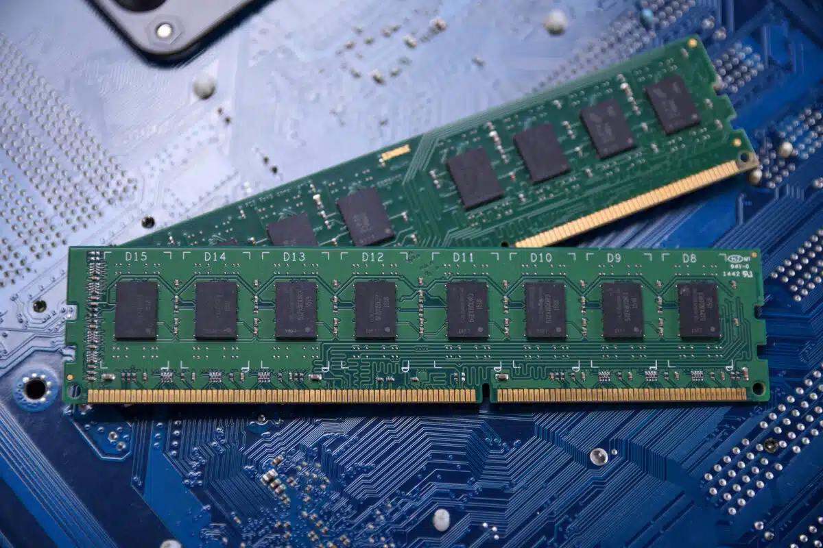

Sourcing Legacy DDR2 & DDR3 Memory in 2026: Supply & Technical Guide

In 2026, the global semiconductor market is experiencing a subtle yet disruptive structural change. While the media prominently highlights next-generation architectures and generative AI, hardware designers and procurement experts working on long-term industrial, networking, and medical platforms encounter a different challenge: a significant shortage in legacy DRAM supply.

Standard dynamic random-access memory platforms such as DDR2 and DDR3 continue to be vital for many embedded systems. However, ensuring the availability of these legacy components has become more challenging,

characterized by ongoing restrictions and significant price fluctuations. To effectively navigate this landscape, engineering and supply chain teams need to comprehend both the macroeconomic factors behind the ongoing legacy shortage and the specific technical limitations influencing memory substitution and integration.

In 2026, the global semiconductor market is experiencing a subtle yet disruptive structural change. While the media prominently highlights next-generation architectures and generative AI, hardware designers and procurement experts working on long-term industrial, networking, and medical platforms encounter a different challenge: a significant shortage in legacy DRAM supply.

Standard dynamic random-access memory platforms such as DDR2 and DDR3 continue to be vital for many embedded systems. However, ensuring the availability of these legacy components has become more challenging, characterized by ongoing restrictions and significant price fluctuations. To effectively navigate this landscape, engineering and supply chain teams need to comprehend both the macroeconomic factors behind the ongoing legacy shortage and the specific technical limitations influencing memory substitution and integration.

Navigate Legacy DRAM Shortages with JSC & ESMT

As legacy memory faces tightening supply, Suntsu provides guaranteed access to industrial-grade DDR2 and DDR3 components through direct partnerships with JSC and ESMT. Secure your production pipeline with reliable, wide-temperature DRAM built for long lifecycle support.

The Legacy Market Landscape

The ongoing supply limitations and abrupt price increases in legacy DRAM technologies stem from semiconductor fabrication reassignments that started in late 2025. This is a documented industry pivot rather than a temporary fluctuation: Samsung is holding firm to its DDR4 end-of-life schedule and SK hynix has signaled plans to phase out DDR4 by 2026, sharply reducing legacy supply [4].

Leading Tier-1 memory manufacturers such as Samsung, SK Hynix, and

Micron have intentionally redirected their advanced wafer capacity from standard, commodity DRAM to focus on producing high-margin components like high-bandwidth memory (HBM) and DDR5 modules. This strategic shift aims to support the surge in infrastructure demand driven by artificial intelligence and high-performance computing (HPC) data centers.

This structural shift has caused a domino effect on older memory generations. As the lead times and prices for DDR5 and DDR4 increased, mid-market OEMs and CMs started redesigning systems based on older architectures like DDR3.

As demand shifted towards the DDR3 market, a second group of buyers downgraded their designs to DDR2. This increase in orders stressed an already fragile supply chain, with only a few dedicated semiconductor design firms and specialty foundries still producing these legacy components.

This cascade is visible in the data. TrendForce reports that as enterprise buyers grew more aggressive in sourcing DDR4 through early 2026, capacity reallocation further tightened DDR3, with high-density DDR3 parts such as 2Gb already in acute shortage and a catch-up price rally taking shape [3].

The surge in demand is further intensified by a supply-side divergence among legacy memory suppliers. Some are reducing older production lines

to focus on higher-density products, while others are maximizing their capacity. This fragile situation compels OEMs and CMs to go beyond standard transactional purchases.

Ensuring the security of programmatic Global Sourcing pipelines and actively managing obsolescence are now critical strategies to safeguard production schedules.

The Legacy Market Landscape

The ongoing supply limitations and abrupt price increases in legacy DRAM technologies stem from semiconductor fabrication reassignments that started in late 2025. This is a documented industry pivot rather than a temporary fluctuation: Samsung is holding firm to its DDR4 end-of-life schedule and SK hynix has signaled plans to phase out DDR4 by 2026, sharply reducing legacy supply [4].

Leading Tier-1 memory manufacturers such as Samsung, SK Hynix, and Micron have intentionally redirected their advanced wafer capacity from standard, commodity DRAM to focus on producing high-margin components like high-bandwidth memory (HBM) and DDR5 modules. This strategic shift aims to support the surge in infrastructure demand driven by artificial intelligence and high-performance computing (HPC) data centers.

This structural shift has caused a domino effect on older memory generations. As the lead times and prices for DDR5 and DDR4 increased, mid-market OEMs and CMs started redesigning systems based on older architectures like DDR3.

As demand shifted towards the DDR3 market, a second group of buyers downgraded their designs to DDR2. This increase in orders stressed an already fragile supply chain, with only a few dedicated semiconductor design firms and specialty foundries still producing these legacy components.

This cascade is visible in the data. TrendForce reports that as enterprise buyers grew more aggressive in sourcing DDR4 through early 2026, capacity reallocation further tightened DDR3, with high-density DDR3 parts such as 2Gb already in acute shortage and a catch-up price rally taking shape [3].

The surge in demand is further intensified by a supply-side divergence among legacy memory suppliers. Some are reducing older production lines to focus on higher-density products, while others are maximizing their capacity. This fragile situation compels OEMs and CMs to go beyond standard transactional purchases.

Ensuring the security of programmatic Global Sourcing pipelines and actively managing obsolescence are now critical strategies to safeguard production schedules.

Architectural Differences between DDR2 and DDR3

When faced with a critical Shortage Mitigation scenario, engineering teams often consider whether the system can be adjusted or backward-integrated with different DDR generations.

The short answer is no. Under the standards established by the Joint Electron Device Engineering Council (JEDEC), DDR2 and DDR3 are fundamentally incompatible on an electrical, physical, and architectural level.

Technical ParameterDDR2 Memory StandardDDR3 Memory Standard
Operating Voltage (VDD)1.8V1.5V (Standard) / 1.35 (DDR3L)
Prefetch Buffer Size4-bit8-bit
Data Rates (Standard)400-1066 MT/s800-2133 MT/s
Internal Bank Structure4 or 8 Banks8 Banks
Signal TerminationOn-Die Termination (ODT)ODT with Dynamic Termination
Physical Form Factor240-Pin DIMM / 200-Pin SO-DIMM240-Pin DIMM / 204-Pin SO-DIMM
Physical Keying / NotchLeft-of-Center AlignmentRight-of-Center, Square Notch

Prefetch Buffer and Core Clock Mechanics

DDR3 attains higher bandwidth mainly through its 8-bit prefetch architecture, which is double the 4-bit prefetch found in DDR2.

In SDRAM architectures, the internal memory array functions significantly slower than the external I/O data bus. The prefetch buffer serves as a high-speed queue:

  • An n-bit prefetch means each internal column access retrieves n data words in a single wide transfer from the slow memory core, which are then streamed out of the I/O buffer at two words per clock cycle — the ‘double data rate’ [1]. DDR2 fetches 4 words per access; DDR3’s 8-bit prefetch fetches 8 [1]. Because the core performs just one access per burst while the I/O serializes the result at two per clock, DDR3 sustains double the external data rate without requiring the internal array to run any faster.

Memory controllers must be specifically programmed to manage these burst structures—generally a fixed burst length of 8 for DDR3, with an on-the-fly chopped burst of 4, versus 4 or 8 for DDR2 [1].

Physical and Electrical Misalignment

DDR2 and DDR3 also differ in nominal operating voltage, and their controllers, signaling, and initialization sequences are mutually unintelligible – a DDR3 controller cannot train or boot a DDR2 module, or vice versa.

To make electrical mismatch impossible in the first place, JEDEC assigns each generation a different keying-notch position, so a module physically cannot seat in the wrong slot [1]. A DDR2 DIMM has a 240-pin layout, but its alignment notch is placed differently from a DDR3 DIMM’s 240-pin layout, physically preventing incorrect insertion.

Latency vs. Bandwidth: Evaluating Real-World Timing Performance

During performance evaluations in a platform redesign or BOM Analysis and Cost Reduction review, engineers typically observe that DDR2 datasheets specify significantly lower Column Address Strobe (CAS) Latency values compared to DDR3.

Indeed, DDR2-800 modules usually have a CAS Latency (CL) of 5 or 6 cycles, while DDR3-1600 modules typically list a CL of 11 cycles. This difference often causes the misconception that DDR2 offers faster initial data access.

In synchronous DRAM, CAS Latency is expressed in clock cycles rather than absolute time units. Since DDR3 runs at much higher clock speeds than DDR2, its clock cycles are considerably shorter.

The actual physical latency in nanoseconds (ns) is calculated using the following formula:

Actual Latency (ns) = CAS Latency (cycles) × Clock Cycle Time (ns)

Using this relationship, we can compare the actual access speeds of DDR2 and DDR3:

DDR2-800 (CL = 5) operating at a 400 MHz I/O clock (2.5 ns clock cycle):

Latency = 5 x 2.5 ns = 12.5 ns

DDR3-1600 (CL = 11) operating at an 800 MHz I/O clock (1.25 ns clock cycle):

Latency = 11 x 1.25 ns = 13.75 ns

Although the absolute latency stays quite similar (between 12 ns and 14 ns), DDR3’s peak transfer bandwidth is twice as high as DDR2’s at the same bus width. This enables the processor to retrieve large amounts of data much more quickly after the initial access delay.

Voltage Compatibility: Operating DDR3 vs. DDR3L

For system designers working on DDR3-based motherboards, managing voltage options is a critical consideration. Standard DDR3 operates at 1.5 V, but JEDEC later defined the DDR3L (Low Voltage) standard, which operates at 1.35 V. DDR3L is defined in Addendum No. 1 to JESD79-3 (JESD79-3-1), which specifies 1.35V operation while preserving compatibility with the 1.5V DDR3 environment [2].

Whether these modules can be interchanged depends heavily on the design of your system’s motherboard and memory controller:

Using DDR3L (1.35V) in a Standard DDR3 (1.5V) System:

This configuration is almost always fully compatible. The JEDEC DDR3L specification requires that low-voltage devices be backward-compatible with standard 1.5V operating environments. When installed in a 1.5V board, the DDR3L memory will safely scale its internal circuits to operate at the higher voltage.

Using Standard DDR3 (1.5V) in a DDR3L (1.35V) System:

This setup is highly problematic and generally fails. If a system controller is designed strictly to output 1.35V to save power, standard 1.5V DDR3 modules will be under-volted. This results in severe signal integrity loss, bit errors, systemic boot failures, or intermittent system crashes under load.

Industrial Grade vs. Consumer Grade

When sourcing Integrated Circuits for industrial automation, medical devices, or critical telecommunications infrastructure, standard consumer-grade RAM is inadequate.

Leading legacy manufacturers like Elite Semiconductor Microelectronics Technology (ESMT) and Jeju Semiconductor Corporation (JSC), distributed by Suntsu, focus on producing industrial-grade DRAM designed to endure harsh environments.

  • Temperature Tolerance: Consumer-grade memory usually specifies a commercial temperature range of 0°C to 70°C. Conversely, industrial-grade components from JSC and ESMT are engineered to operate within the industrial temperature range of -40°C to 85°C, with some extended up to 105°C for automotive applications.
  • Silicon Longevity: Consumer DRAM components typically have short lifecycles, becoming obsolete in about 18 to 24 months. In contrast, specialized industrial suppliers offer extended lifecycle support programs, ensuring production availability for 7 to over 10 years to avoid the need for forced redesigns.
  • Failures in Time (FIT) Rates: Industrial silicon is subjected to thorough testing, such as Burn-In and specialized screening, to reduce infant mortality and lower overall FIT rates under continuous operational stress.

Error-Correcting Code (ECC) Support in High-Reliability Applications

For important deployments like aerospace, medical imaging, or industrial SCADA nodes, ensuring data integrity is essential.

DDR3 includes support for Error-Correcting Code (ECC), which employs extra data lines—usually an additional 8 bits on a 64-bit bus—leading to a total physical bus width of 72 bits to convey parity information.

This architecture enables the memory controller to immediately identify and correct single-bit errors and detect multi-bit errors, the former often caused by cosmic rays, magnetic interference, or background radiation. These single-event upsets are a well-characterized reliability concern with their own JEDEC measurement standard, JESD89A, which defines how alpha-particle and terrestrial cosmic-ray soft-error rates are tested and reported for semiconductor devices [5].

When setting up your platform, it is crucial to choose memory controllers and processors that explicitly support ECC protocols, since typical consumer-grade chipsets usually disable these features.
Mitigating Sourcing Risks: Suntsu’s Active Legacy Pipeline

Since legacy allocation constraints remain, ensuring an uninterrupted manufacturing process depends on having dependable, direct supply chains.

Suntsu Electronics functions with a hybrid business model, acting as both a custom manufacturer and an independent distributor supported by an extensive global partner network. The company maintains active memory allocation and consistent inventory pipelines for DDR2 and DDR3.

Through our distribution agreements and sourcing partnerships with top-tier specialty memory producers such as ESMT and Jeju Semiconductor Corporation (JSC), we provide immediate support for complex bills of materials.

Whether your team needs assistance in finding drop-in industrial replacements, handling EOL transitions, or adopting long-term Inventory Management Solutions, Suntsu provides the technical expertise and supply chain reliability essential for maintaining your production lines.

Don’t let legacy memory allocation delays stall your production lines. Contact Suntsu’s engineering and supply chain experts today to secure DDR2 and DDR3 inventory for your project.

FAQs

No. Mixing ECC and non-ECC modules on the same channel is generally not supported. Most memory controllers will either fail to complete POST or will automatically disable ECC functionality across all installed memory, falling back to non-ECC mode. For high-reliability industrial systems requiring parity checking, all populated modules must support ECC.

DDR2 monolithic chip densities typically max out at 2Gb per die, whereas DDR3 scales up to 8Gb per die. When selecting drop-in replacements from specialty suppliers like ESMT or JSC, engineers must verify that the existing memory controller or system-on-chip (SoC) supports the specific addressing structure (row, column, and bank address bits) of higher-density monolithic dies, as older SoCs often cannot address high-density chips correctly.

  • UDIMM (Unbuffered DIMM): The standard module type used in most desktop and embedded boards; signals drive directly from the controller to the DRAM chips.

  • RDIMM (Registered DIMM): Contains a register hardware buffer between the memory controller and the DRAM chips to reduce electrical loading on the system bus, primarily used in enterprise servers and high-density industrial platforms.

  • SO-DIMM (Small Outline DIMM): A compact physical form factor (~half the size of standard DIMMs) designed for space-constrained embedded systems and handheld computers.

DDR2 operates at 1.8V compared to DDR3’s 1.5V/1.35V, requiring higher baseline current consumption. Additionally, DDR2 lacks the refined dynamic power management and termination state controls found in DDR3. In fanless or sealed industrial enclosures operating at high ambient temperatures (>70°C), DDR2 modules require careful board layout trace spacing, thermal vias, or active airflow to prevent thermal throttling and data retention errors.

DDR2 uses SSTL_18 (Stub Series Terminated Logic 1.8V), whereas DDR3 uses SSTL_15 (1.5V). The lower voltage threshold in SSTL_15 reduces overall power consumption and noise generation, enabling clean signaling at the higher clock speeds required for DDR3’s double-digit gigabyte transfer rates.

References

[1] JEDEC. “JESD79-3 DDR3 SDRAM Standard” Available at: https://www.jedec.org/standards-documents/docs/jesd-79-3d
[2] JEDEC. “DDR3L Low Voltage Memory Standard announcement” Available at: https://www.jedec.org/news/pressreleases/jedec-publishes-widely-anticipated-ddr3l-low-voltage-memory-standard
[3] Trendforce. “DDR4 Reportedly Leads Legacy Memory Rally with Q1 Prices Up to 50%; DDR3 in Tight Supply” Available at: https://www.trendforce.com/news/2026/01/19/news-ddr4-reportedly-leads-legacy-memory-rally-with-q1-prices-up-to-50-ddr3-in-tight-supply/
[4] Trendforce. “Out with the Old: Memory Giants Map Their 2025-26 Exit Strategy amid Supply Crunch” Available at: https://www.trendforce.com/news/2026/01/19/news-out-with-the-old-memory-giants-map-their-2025-26-exit-strategy-amid-supply-crunch/
[5] JEDEC. “JESD89A Soft Error Measurement Standard” Available at: https://www.jedec.org/standards-documents/docs/jesd-89a

keyboard_arrow_up