
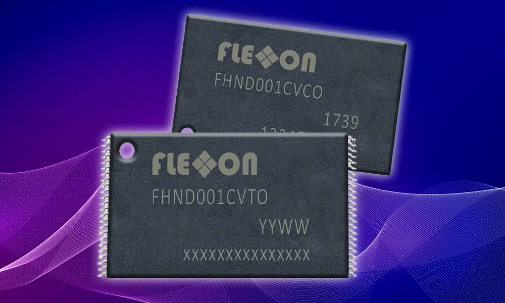

How NAND Flash Memory Works
At a technical level, NAND flash memory organizes its cells into pages, which are then grouped into blocks. Due to this design, data must be written and read one page at a time but erased in larger block units. This structure, named “NAND” after the “Not AND” gate, enables higher storage density and reduces the cost per bit compared to NOR flash, helping drive the evolution of modern NAND technology. Unlike random-access memory, NAND flash stores data in tightly packed memory cells organized in blocks, which allows for high storage density but introduces tradeoffs in write and erase behavior.
When an engineer chooses a NAND component, they assess the condition of electrons trapped inside a tiny insulator. Over time, these cells degrade because of the high-voltage stress needed to program and erase them. The mechanism is physical: repeated high-voltage program and erase operations wear the insulating tunnel oxide, which is what places a finite ceiling on P/E cycles [1]. This is when reliability metrics like Program/Erase (P/E) cycles are essential. For a comprehensive comparison of these architectures, our NOR Flash Guide 2026: Architecture, reliability, and NAND vs NOR provides valuable insights for those weighing design performance against durability.
3D NAND Flash Memory: Advancing Storage Density Beyond Planar Limits
3D NAND was developed to overcome the scaling limits of planar NAND, where shrinking memory cells further would negatively impact reliability and endurance. Instead of reducing cell size, 3D NAND introduces layers of memory cells stacked vertically, enabling significantly higher storage density while relaxing rather than tightening the reliability constraints, since 3D stacking let manufacturers step back to a larger, more forgiving process node instead of shrinking cells further [1].
Advances in 3D NAND have increased storage density and performance, making NAND flash essential for devices like SSDs, memory cards, and USB flash drives.
Where NAND Flash is used
The versatility of NAND flash has cemented its place in nearly every sector of the technology industry.

NAND flash is the key technology behind everything from basic USB drives to top-tier enterprise SSDs. These devices utilize high-density NAND to store enormous amounts of data, supported by advanced controllers that perform error correction and wear leveling. For readers keen on understanding the performance differences among these storage options, our SSD Deep Dive: NVMe, NAND Flash, and Performance offers a detailed explanation of how these technologies interact with modern systems.
In embedded environments like automotive dashboards or IoT gateways, NAND memory offers the storage capacity needed for complex operating systems and firmware. Since embedded designs often last several years, choosing a supplier with a stable roadmap is crucial to prevent costly re-qualification of components. For effective management of these designs, consulting Memory IC essentials: selecting the right components for your project can simplify your initial component selection process.
Industrial applications are among the most demanding for NAND flash, operating in harsh environments with extreme temperatures, high vibration, and frequent power cycling, which can accelerate cell degradation. Consumer-grade components often fail under these conditions. To address this, high-end industrial modules like those from our partner Flexxon are specially designed with improved error correction and specialized NAND architecture to endure these challenges. Furthermore, authorized manufacturing partners such as ESMT and JSC provide exceptionally reliable memory and NAND flash products designed to accommodate a wide variety of rigorous industrial and embedded storage needs.
How to Choose the Right NAND Flash
Selecting the correct NAND component is a balance of engineering requirements and procurement realities. Understanding the different types of NAND flash can help engineers and procurement teams choose the right balance of performance, endurance, and cost for their application.
Capacity & Performance
Engineers need to determine the total storage requirements and required throughput (IOPS). Procurement should review these estimates early to confirm that the selected capacities are not allocated elsewhere. If market fluctuations are causing pressure, our recent analysis in NAND Flash Price Surge offers practical insights for managing these budget-conscious choices.
Endurance & Reliability
Endurance is more than just a specification; it acts as a fundamental design constraint. If your application involves continuous data writing, it’s essential to consider the P/E cycle limits associated with different NAND types, such as SLC, MLC, TLC, or QLC. For comparing finished drives rather than raw die, JEDEC’s JESD218 defines a standardized SSD Endurance Rating expressed in terabytes written (TBW), which lets you evaluate parts from different manufacturers on a common basis [2]. Critically, the standard defines two application classes — Client and Enterprise — with different active-use and data-retention requirements, so a TBW figure is only meaningful against the class your application actually matches [2]. An industrial design specified against a client-class rating is a common and expensive mistake. For teams aiming to plan the long-term development of their products, gaining an understanding of the broader technological shifts is crucial. We suggest reviewing The Future of MLC NAND: Understanding Market Shifts and Sourcing Alternatives to remain informed about component trends.
Lifecycle & Availability
The biggest mistake during the design phase is choosing a component without confirming its lifecycle status. A component that works perfectly now could cause major issues later if it reaches EOL, requiring a redesign or urgent procurement of aftermarket parts. Proactive sourcing is essential to reduce the risk of unexpected EOL notices that could delay a project launch.

The Role of NAND Flash in Modern Systems
NAND flash technology forms the backbone of modern data systems, but its effectiveness depends on a reliable supply chain. For engineers, it concerns specifications and architecture; for purchasing managers, it involves lead times and managing risks. In practice, NAND flash selection is as much about ensuring supply continuity and lifecycle stability as it is about meeting performance and capacity requirements.
At Suntsu Electronics, we help you seamlessly connect design and delivery. Whether offering independent distribution for legacy requirements or supporting comprehensive BOM analysis and cost reduction, our specialists are dedicated to keeping your projects on schedule and within budget. Don’t let supply chain disruptions affect your profits—reach out to our team today for advice on your next project’s storage plan.
Whether you need expert guidance navigating complex storage architectures or a resilient supply chain partner to mitigate EOL risks, Suntsu is ready to seamlessly connect your design with delivery. Request a quote today to secure your required NAND flash components and keep your project on schedule.
FAQs
These terms refer to the number of bits stored in a single memory cell. SLC (Single-Level Cell) stores 1 bit, MLC (Multi-Level Cell) stores 2, TLC (Triple-Level Cell) stores 3, and QLC (Quad-Level Cell) stores 4. Storing more bits per cell requires the controller to distinguish between more voltage states (e.g., QLC requires 16 distinct voltage levels). As bit density increases, storage capacity goes up and cost per gigabyte goes down, but write speeds and overall endurance (P/E cycles) significantly decrease.
Over time, the electrical charge trapped inside a NAND cell can leak or be disturbed by neighboring cell activity, leading to “bit flips” where a 0 becomes a 1, or vice versa. As memory geometries shrink and more bits are packed into each cell, the voltage margins become razor-thin. Advanced ECC algorithms (like LDPC or BCH) run constantly on the memory controller to detect and correct these hardware-level errors on the fly, ensuring data integrity.
Both are technologies used to trap electrons and store data. Traditional floating-gate technology uses a conductive polysilicon layer to hold electrons. Charge-trap technology, on the other hand, uses a thinner, insulating silicon nitride layer. Because the charge-trap layer is an insulator, it is much less prone to electron leakage and can be manufactured much thinner. This is why charge trap underpins nearly all 3D NAND: a floating gate is extremely difficult to pattern vertically, since lithography works from the top down, while a charge trap layer needs no patterning at all [3].The one exception is the 3D floating-gate NAND developed by the Intel–Micron joint venture; Micron abandoned the approach in 2020, leaving SK Hynix’s Solidigm as its only remaining user [3].
Because the insulating oxide layer in a NAND cell physically degrades every time an erase voltage is applied, cells have a finite lifespan. Wear leveling is an algorithm managed by the memory controller that maps logical block addresses to physical block addresses. It ensures that data writes are distributed evenly across all physical blocks on the chip, rather than repeatedly overwriting the same physical sector, thereby extending the overall lifespan of the module.
While NAND flash offers incredible density and is non-volatile, its architecture is fundamentally different from DRAM (Dynamic Random Access Memory). NAND must write data in “pages” and erase data in massive “blocks,” whereas DRAM allows for true byte-level random access. Furthermore, NAND read/write latencies are measured in microseconds, whereas DRAM operates in nanoseconds—orders of magnitude faster and without the physical degradation caused by P/E cycles.
Related Content
References
[1] Cai, Ghose, Haratsch, Luo & Mutlu, “Errors in Flash-Memory-Based Solid-State Drives: Analysis, Mitigation, and Recovery” Available at: https://arxiv.org/pdf/1711.11427
[2] JEDEC, “JESD218 (SSD Requirements and Endurance Test Method) and JESD219 (SSD Endurance Workloads)” Available at: https://www.jedec.org/standards-documents/focus/flash/solid-state-drives
[3] Jim Handy, The Memory Guy “3D NAND: Making a Vertical String” Available at: https://thememoryguy.com/3d-nand-making-a-vertical-string/
[4] TrendForce, “Contract Prices Surged More Than 100% in 1H26; Structural Shortages to Keep NOR Flash and SLC NAND Prices Rising in 2H26, Says TrendForce” Available at: https://www.trendforce.com/presscenter/news/20260616-13102.html