
 Managing modern multi-rail architectures requires strict coordination across distinct voltage boundaries. Complex system-on-chip (SoC) devices, field-programmable gate arrays (FPGAs), microcontrollers (MCUs), and microprocessors rely on separate power rails to balance high-speed core processing with flexible input/output (I/O) communication. When these supply lines do not energize in the proper order, current can flow through unintended parasitic paths inside the silicon die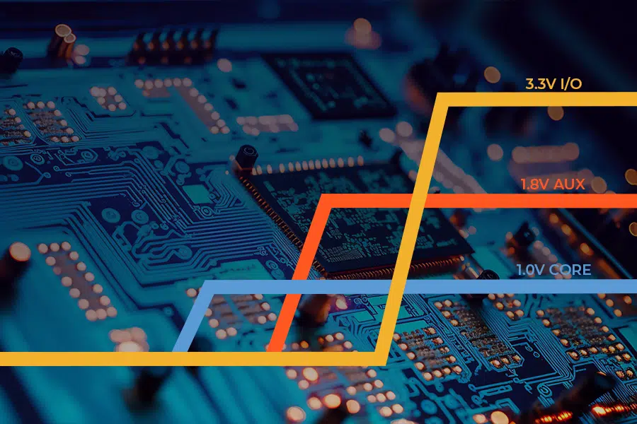
What Is Power Sequencing and Why It Matters
 Power sequencing governs the precise time delays and voltage relationships between multiple power rails in an integrated circuit during startup and shutdown. Modern digital processing ICs require distinct supply voltages: a lower voltage core rail (often 0.8V to 1.2V) to run dense logic gates, and higher voltage rails (such as 1.8V, 2.5V, or 3.3V) to drive off-chip I/O interfaces.
Risks of Incorrect Sequencing

Latch-Up Conditions
Latch-up is an inadvertent low-impedance path created between a power rail and ground, triggering a short-circuit condition driven by parasitic silicon-controlled rectifier (SCR) structures inside CMOS devices. When an I/O voltage rail powers on while the core supply remains unenergized, input signals can inject current into the substrate through internal protection diodes. This current triggers the parasitic PNP and NPN transistors within the CMOS substrate, creating a self-sustaining feedback loop that draws excessive current until power is removed or the silicon suffers physical damage[4][5].

Component Stress and Damage
Uncontrolled voltage differences across internal transistor terminals create severe electric field stress across gate oxide layers. Over time, or even during a single unsequenced power cycle, this overvoltage stress can degrade the die and cause premature component failure. Manufacturers often specify limits here. AMD, for instance, caps how long certain I/O and auxiliary rails may differ by more than a set voltage during each power cycle to maintain reliability[3]. Furthermore, uncontrolled inrush current into uncharged rail capacitors can trip upstream current limits, cause input voltage droop, and stress connectors and protection components. Staggering rail turn-on spreads that inrush over time, which is especially helpful with current-limited supplies[1].

Data Corruption on Digital Rails
Incomplete logic state definitions during power transients can corrupt non-volatile flash devices, external memory modules, and internal configuration registers. If an active communication bus powered by an I/O rail attempts to drive data into a processor whose core rail is partially energized, indeterminate voltage levels on control or bus lines can be misread as valid logic states, triggering spurious writes or resets. This glitching leads to boot failures, corrupted system registers, and unpredictable firmware execution.
Sequencing Methods
Architects select power supply sequencing implementations based on system complexity, bill of materials (BOM) cost limits, and timing accuracy requirements. The choice typically falls between passive discrete networks and dedicated integrated controllers.
Discrete RC/Diode-Based Sequencing
Discrete networks use resistor-capacitor (RC) delays combined with Schottky diodes or simple bipolar junction transistors to stagger enable lines across sequential regulators. As the first regulator output rises, it charges the downstream capacitor through an RC network until reaching the threshold voltage of the next stage’s enable input. While inexpensive, discrete RC delay circuits are highly sensitive to passive component tolerances, temperature drift, and supply fluctuations. They also fail to monitor whether a prerequisite rail has actually reached nominal regulation before enabling the subsequent stage[1][6].
Dedicated Power Sequencer ICs
Dedicated power sequencing ICs combine a voltage sequencer and supervisor to deliver robust, multi-channel supervision by actively measuring each voltage rail using internal analog comparators. A power sequencer delays the activation of subsequent power channels until real-time measurement confirms all upstream rails sit firmly within defined operating thresholds. Modern sequencers allow hardware engineers to set delay times, monitor fault conditions, and execute controlled power-down sequences. With digitally configured sequencers, the rail order can be changed in firmware rather than with a PCB layout change[7][8]. For sophisticated systems utilizing advanced processors, integrating the sequencing function into dedicated power management ICs simplifies timing configurations while reducing discrete component counts.
Sequencing Method Timing Accuracy Fault Monitoring Board Area Relative Cost Discrete RC / Diode Low (Tolerances / Temp Drift) None Medium Lowest PGOOD-Gated Daisy Chain Medium (Threshold Dependent) Basic Output Checking (No Native Power-Down Control) Small Low Power Sequencing IC High (Fixed or Programmable Delays) Advanced Over/Under Voltage Compact Moderate
Power-Up vs. Power-Down Sequencing Requirements
Ramp-Up Order and Timing
Selecting the correct ramp-up order depends on the sequencing requirements specified in the device manufacturer’s datasheet. Many FPGAs, SoCs, and processors specify a core-first strategy[1][3], where internal logic rails must stabilize before external I/O rails energize. Conversely, some devices specify a different order, such as I/O or analog rails first, so always confirm against the datasheet[1][7]. Timing parameters such as rail ramp rates (dV/dt) and minimum dwell times between stages must be validated using specialized board design and circuit analysis to confirm there is no current back-feeding during initialization.
Controlled Shutdown Considerations
Power-down sequencing is equally critical to long-term system health. During sudden power loss or system standby transitions, failing to discharge high-voltage I/O rails before core logic collapses can drive residual charge back through ESD structures into the collapsing rail. Controlled shutdown sequences commonly run in the reverse of the power-up order[3], though some device families specify otherwise, so check the datasheet[6]. Active discharge circuitry built into many regulators, sequencers, and PMICs bleeds off bulk storage capacitors quickly, ensuring all power nodes discharge to near zero volts before the system re-energizes.
Working with PGOOD/Enable Pins for Sequencing Control
 Many switching regulators and
 Design Checklist for Multi-Rail Sequencing
To ensure first-pass success when designing multi-rail power distribution networks, run through this design review sequence:
- Review Datasheet Timing Specifications: Identify explicit power-up and power-down sequencing charts, dV/dt ramp rate limits, and maximum allowed voltage differences between rails[3].
- Calculate Inrush Currents: Verify that input bulk capacitance and regulator soft-start rise times keep peak inrush current below trace, connector, and upstream supply current limits.
- Map the Enable Architecture: Decide whether discrete RC delays, PGOOD daisy-chaining, or a dedicated power sequencing IC offers the required timing precision and fault detection coverage.
- Implement Active Discharge Controls: Verify that bulk capacitors on all rails fully discharge during shutdown to prevent stuck logic levels on warm restarts.
- Analyze Thermal and Signal Integrity: Ensure layout routing places power control circuits away from high-temperature power inductors and high-speed clock paths. If custom pinouts or compact layouts are necessary, leverage specialized custom electronic components to consolidate power management blocks.
- Simulate Transient and Fault Scenarios: Evaluate system behavior when an intermediate rail drops out unexpectedly due to an overcurrent fault, and confirm whether the sequencer shuts down all rails or only dependent ones.
Getting Multi-Rail Sequencing Right
Power sequencing is easy to overlook until a board fails to boot or a device latches up on the bench. Whether you choose discrete RC delays, a PGOOD daisy chain, or a dedicated power sequencing IC, the right approach starts with the device datasheet and accounts for both power-up and power-down behavior. When designing complex multi-rail power supplies, navigating rail layout trade-offs and component selection requires deep technical expertise. Suntsu’s experienced engineering team offers complete component engineering support to help you analyze schematics, qualify drop-in alternatives, and resolve difficult power delivery challenges.
Ready to finalize your power architecture? Contact Us to have our engineers review your multi-rail design, or Get a Quote on high-reliability power management components.
FAQs
Check the Absolute Maximum Ratings table. A rating like “pin X must stay within VDD + 0.3V” tells you which supply has to come up first. In the AD7654 example, OVDD can be at most 0.3V above DVDD, so DVDD has to power up before or together with OVDD. Powering OVDD first would violate the rating and could damage the part[7].
Yes. If an analog signal or reference is present before AVDD, the analog core is very likely to power up latched. This is usually nondestructive, but AVDD current can climb to about ten times normal and make the ADC hot. The fix is to sequence the ADC with its inputs and reference unpowered or disconnected[7].
Sequencing turns rails on and off in a set order. Tracking controls how rails rise relative to each other. There are three kinds of tracking: coincident, ratiometric, and offset. In coincident tracking, all supplies start together and rise at the same rate, so the lower voltages are reached before the higher ones[11].
Often, if they have the same voltage. For Spartan-7, VCCINT and VCCBRAM can share a supply and ramp together if their recommended voltages match, and the same goes for VCCAUX and VCCO[3].
Related Content
References
- J. Espiritu. “Complex Power-Supply Sequencing Made Easy” Available at: https://www.analog.com/en/resources/analog-dialogue/articles/complex-power-supply-sequencing.html
- D. Walther. “ESD Diode Current Specification” Available at: https://www.ti.com/lit/pdf/slaa689
- AMD. “Power-On/Off Power Supply Sequencing” Available at: https://docs.amd.com/r/en-US/ds189-spartan-7-data-sheet/Power-On/Off-Power-Supply-Sequencing
- JEDEC. “JESD78F.02: IC Latch-Up Test” Available at: https://www.jedec.org/node/8529
- M. Johnson, R. Cline, S. Ward, and J. Schichl. “Latch-Up” Available at: https://www.ti.com/lit/pdf/scaa124
- C. Wallace. “FPGA Power Made Simple: Sequencing” Available at: https://www.ti.com/lit/pdf/sszt890
- C. Augusta and M. Murnane. “Power Supply Sequencing” Available at: https://www.analog.com/en/app-notes/an-932.html
- Texas Instruments. “Power-Supply Sequencing for FPGAs” Available at: https://www.ti.com/lit/slyt598
- Texas Instruments. “TPS7A84 Datasheet (SBVS233B)” Available at: https://www.ti.com/lit/ds/symlink/tps7a84.pdf
- Texas Instruments. “TPSM84A21 Datasheet (SLVSDF7A)” Available at: https://www.ti.com/lit/ds/symlink/tpsm84a21.pdf
- ADI Analog Dialogue “Monitoring and Sequencing in Multirail Power-Supply Systems” Available at: https://www.analog.com/en/resources/analog-dialogue/articles/monitoring-and-sequencing-multirail-power-supply-sys.html