
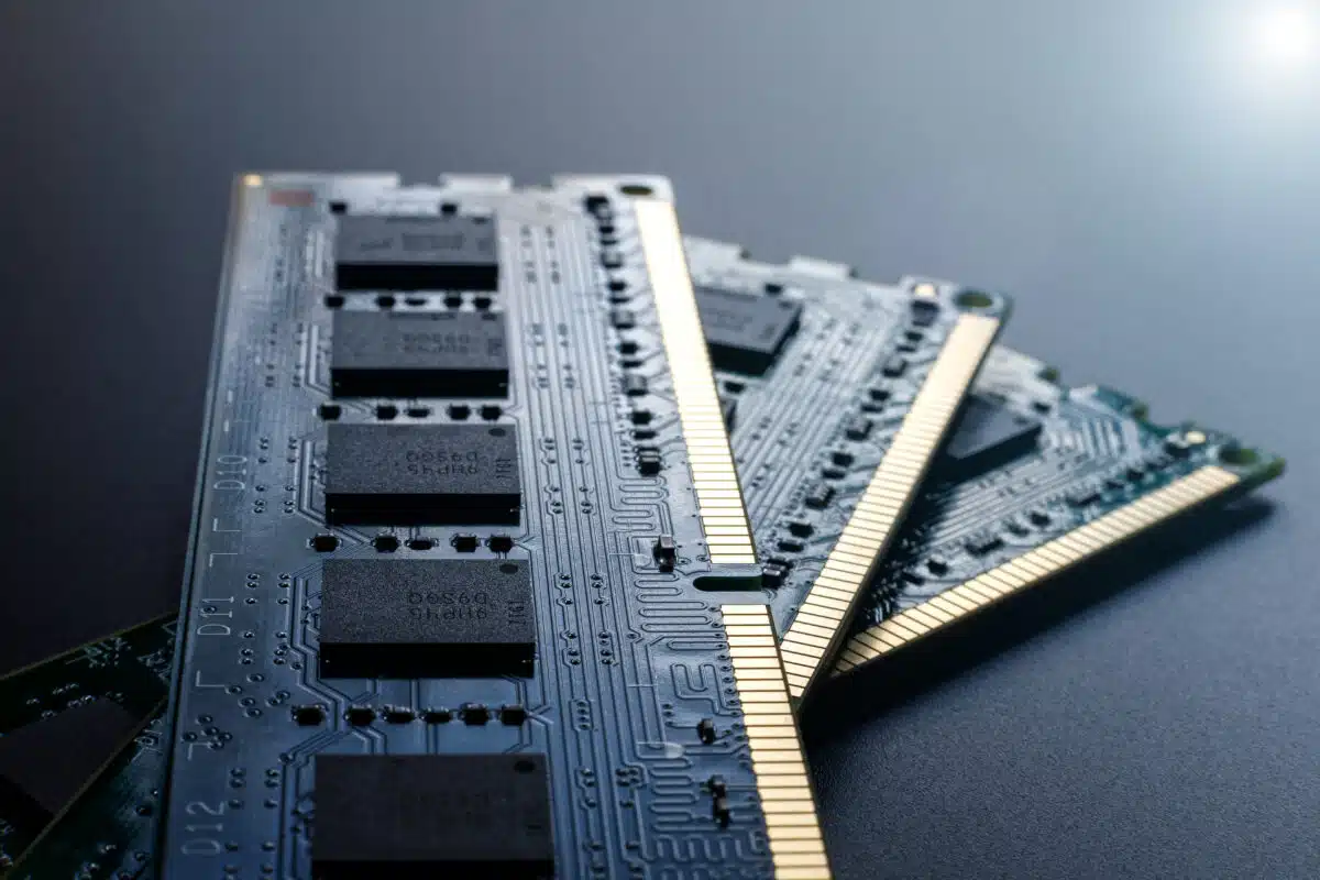
DRAM Refresh Cycles and Power Management: What Engineers Overlook

DRAM refresh is the mandatory background operation of periodically recharging the internal storage capacitors within dynamic random-access memory cells to prevent data loss due to charge leakage. Because DRAM specifications only guarantee that cells hold their charge for tens of milliseconds (DDR4 requires every cell to be refreshed at least every 64 ms at normal operating temperatures), refresh runs continuously and accounts for a meaningful share of memory power: around 20% of DRAM power at 16 Gb densities, with projections approaching 50% as densities climb[1][2][3]. That overhead creates thermal and battery life challenges in power-sensitive designs.

When evaluating memory architectures, hardware development teams routinely calculate system power based on active read and write operations. They often treat idle memory states as near-zero power drawers, missing the steady baseload current drawn by DRAM Memory. In duty-cycled, edge-computing, and high-temperature environments, this baseline can become one of the largest contributors to the memory subsystem’s energy budget, particularly during long standby periods.

Managing memory power efficiency requires looking beyond baseline read and write currents. Understanding how internal refresh commands execute across active and idle states, how elevated thermal conditions accelerate capacitor charge decay, and how firmware controls can mitigate refresh overhead allows engineers to design reliable, energy-efficient hardware.

DRAM refresh is the mandatory background operation of periodically recharging the internal storage capacitors within dynamic random-access memory cells to prevent data loss due to charge leakage. Because DRAM specifications only guarantee that cells hold their charge for tens of milliseconds (DDR4 requires every cell to be refreshed at least every 64 ms at normal operating temperatures), refresh runs continuously and accounts for a meaningful share of memory power: around 20% of DRAM power at 16 Gb densities, with projections approaching 50% as densities climb[1][2][3]. That overhead creates thermal and battery life challenges in power-sensitive designs.

When evaluating memory architectures, hardware development teams routinely calculate system power based on active read and write operations. They often treat idle memory states as near-zero power drawers, missing the steady baseload current drawn by DRAM Memory. In duty-cycled, edge-computing, and high-temperature environments, this baseline can become one of the largest contributors to the memory subsystem’s energy budget, particularly during long standby periods.

Managing memory power efficiency requires looking beyond baseline read and write currents. Understanding how internal refresh commands execute across active and idle states, how elevated thermal conditions accelerate capacitor charge decay, and how firmware controls can mitigate refresh overhead allows engineers to design reliable, energy-efficient hardware.

Key Takeaways

  • Dynamic memory storage capacitors continuously leak charge, requiring mandatory periodic refresh cycles to maintain data retention across the array[2].
  • Higher operating temperature accelerates charge leakage, so DDR4 specifications require refresh rates to double once the DRAM case temperature exceeds 85°C, with further increases for automotive-grade parts[1][4][5].
  • Partial-Array Self-Refresh (PASR) reduces idle self-refresh power consumption by refreshing only the memory banks or segments that hold data that must be retained[6][7].
  • Refresh current during active operation (listed as IDD5B, “burst refresh current,” in DDR datasheets) adds repetitive current pulses, while self-refresh current (IDD6) sets the memory’s standby power floor and rises steeply with temperature[6][8].
  • Temperature-compensated self-refresh lowers standby current when the die is cool, while controller-level refresh scheduling reduces latency penalties in high-density memory designs[2][12].

Find Memory Built for Your Power Budget

Refresh overhead varies widely across DRAM types, densities, and temperature grades. Explore Suntsu’s DRAM portfolio to compare low-power and industrial-grade options for your next design.

Why Does DRAM Require Continuous Refreshing to Store a Bit?
DRAM requires continuous refreshing because each tiny cell capacitor, paired with a single access transistor, must store a bit of data as an electrical charge (1T1C architecture)[2]. Unlike static RAM (SRAM), which uses multi-transistor bistable latches to retain data indefinitely as long as power is applied, a DRAM storage capacitor is inherently lossy.  The capacitor constantly discharges through subthreshold leakage in the access transistor, junction leakage at the storage node, and tunneling currents such as gate-induced drain leakage (GIDL)[3].

Volatile memory behavior dictates that without active intervention, the voltage level on a charged capacitor decays below the threshold required for sense amplifiers to distinguish between a logical high (1) and a logical low (0). Most cells can actually store their data for seconds or longer, but the refresh schedule has to protect the leakiest cells in the device[2][9]. To prevent bit flips and data corruption, every row must therefore be recharged within a specified refresh window: 64 ms for DDR4 at normal operating temperatures, or 32 ms for LPDDR4[1][10]. The controller spreads this work

across 8,192 REFRESH commands issued at an average interval known as tREFI, about 7.8 µs for DDR4[1].

During a DRAM refresh operation, the row decoder activates a word line, exposing the capacitor charge to the bit line. The sense amplifier detects the minute voltage shift and amplifies it, driving the bit line fully to the supply voltage or to ground, which restores the cell to a full “1” or “0” before the row is closed[2]. Because every row must be recharged within each refresh window, and a single 8 Gb chip contains more than 500,000 rows holding billions of cells[3], refresh incurs continuous power overhead regardless of whether the processor is actively accessing the memory Integrated Circuits.

DRAM requires continuous refreshing because each tiny cell capacitor, paired with a single access transistor, must store a bit of data as an electrical charge (1T1C architecture)[2]. Unlike static RAM (SRAM), which uses multi-transistor bistable latches to retain data indefinitely as long as power is applied, a DRAM storage capacitor is inherently lossy.  The capacitor constantly discharges through subthreshold leakage in the access transistor, junction leakage at the storage node, and tunneling currents such as gate-induced drain leakage (GIDL)[3].

Volatile memory behavior dictates that without active intervention, the voltage level on a charged capacitor decays below the threshold required for sense amplifiers to distinguish between a logical high (1) and a logical low (0). Most cells can actually store their data for seconds or longer, but the refresh schedule has to protect the leakiest cells in the device[2][9]. To prevent bit flips and data corruption, every row must therefore be recharged within a specified refresh window: 64 ms for DDR4 at normal operating temperatures, or 32 ms for LPDDR4[1][10]. The controller spreads this work across 8,192 REFRESH commands issued at an average interval known as tREFI, about 7.8 µs for DDR4[1].

During a DRAM refresh operation, the row decoder activates a word line, exposing the capacitor charge to the bit line. The sense amplifier detects the minute voltage shift and amplifies it, driving the bit line fully to the supply voltage or to ground, which restores the cell to a full “1” or “0” before the row is closed[2]. Because every row must be recharged within each refresh window, and a single 8 Gb chip contains more than 500,000 rows holding billions of cells[3], refresh incurs continuous power overhead regardless of whether the processor is actively accessing the memory Integrated Circuits.

How Do Auto-Refresh, Self-Refresh, and PASR Modes Compare?

Managing power consumption in dynamic memory relies on selecting the appropriate refresh operational mode based on the current workload state of the system. Memory standards, including DDR4, DDR5, and low-power variants like LPDDR4x Memory Modules, define distinct modes for balancing data retention, access latency, and power dissipation.

The standard operational state is auto-refresh, sometimes still called CAS-before-RAS (CBR) refresh after the asynchronous DRAM scheme it descends from[2]. In this mode, the host clock remains active and the memory controller periodically issues REFRESH commands; the DRAM’s internal counter selects which rows to refresh, so the controller never has to send row addresses[2]. Auto-refresh is used during active system states. Its current is characterized in DDR datasheets as burst refresh current (IDD5B), and because the clock, input receivers, and interface logic stay powered, it costs more than self-refresh[2][8]. In DDR3 and DDR4, each REFRESH command also blocks access to every bank on the rank for the duration of the command (tRFC)[2].

When the system enters low-power or sleep modes, the memory transitions to Self-Refresh. The host can stop the external clock (CK), and the memory device uses an internal timer for autonomous DRAM refresh cycles while its DLL, clock receivers, and I/O are shut down[8][11]. This mode eliminates interface clocking power and reduces current draw to self-refresh levels (IDD6)[2]. The trade-off is wake-up time: exiting self-refresh takes far longer than exiting a standard power-down mode[2].

To further optimize battery-operated equipment, Partial-Array Self-Refresh (PASR), a JEDEC power-saving feature found mainly in low-power LPDDR memory, lets firmware mask unused banks or segments from self-refresh; data in the masked regions is not retained[7][11][12]. If an application needs only a quarter of the memory during standby, PASR can limit refresh to that quarter. The savings are substantial but not strictly proportional, because peripheral circuits and leakage keep drawing current, so check the partial-array IDD6 values in the device datasheet[2][13].

When the system enters low-power or sleep modes, the memory transitions to Self-Refresh. The host can stop the external clock (CK), and the memory device uses an internal timer for autonomous DRAM refresh cycles while its DLL, clock receivers, and I/O are shut down[8][11]. This mode eliminates interface clocking power and reduces current draw to self-refresh levels (IDD6)[2]. The trade-off is wake-up time: exiting self-refresh takes far longer than exiting a standard power-down mode[2].

To further optimize battery-operated equipment, Partial-Array Self-Refresh (PASR), a JEDEC power-saving feature found mainly in low-power LPDDR memory, lets firmware mask unused banks or segments from self-refresh; data in the masked regions is not retained[7][11][12]. If an application needs only a quarter of the memory during standby, PASR can limit refresh to that quarter. The savings are substantial but not strictly proportional, because peripheral circuits and leakage keep drawing current, so check the partial-array IDD6 values in the device datasheet[2][13].

Refresh ModeExecution StatePower Consumption ImpactPrimary Application Use Case
Auto-refreshDriven by host memory controller via explicit commands while system clock (CK) is active.Highest; burst refresh current (IDD5B) adds to active power, and each REFRESH command blocks the target banks for rRFC[2][8]Fully operational system states with continuous CPU access and high throughput tasks.
Self-refreshAutonomous operation using internal chip oscillator; host system clock is gated off.Medium-low (IDD6 idle current); eliminates interface, clock tree, and input buffer power draw.System standby, sleep, or low-power operational modes where memory content must be preserved.
Partial-Array Self-Refresh (PASR)On-chip timer refreshes only designated banks or segments (e.g., 1/2, 1/4, or 1/8 of the array); data in masked regions is lost[7][13].Lowest standby power; falls as less of the array is refreshed, but not in strict proportion because peripheral and leakage currents remain[2][13].Battery-powered embedded devices, duty-cycled sensors, and wearable systems keeping minimal kernel data alive.

Selecting the optimal mode requires balancing system wake-up latency against static power targets. While PASR can provide substantial energy savings during extended sleep cycles, software architectures must carefully segregate volatile retention buffers into designated memory banks to prevent data loss in non-refreshed areas.

What Is the Practical Impact of Temperature on DRAM Refresh Rates?
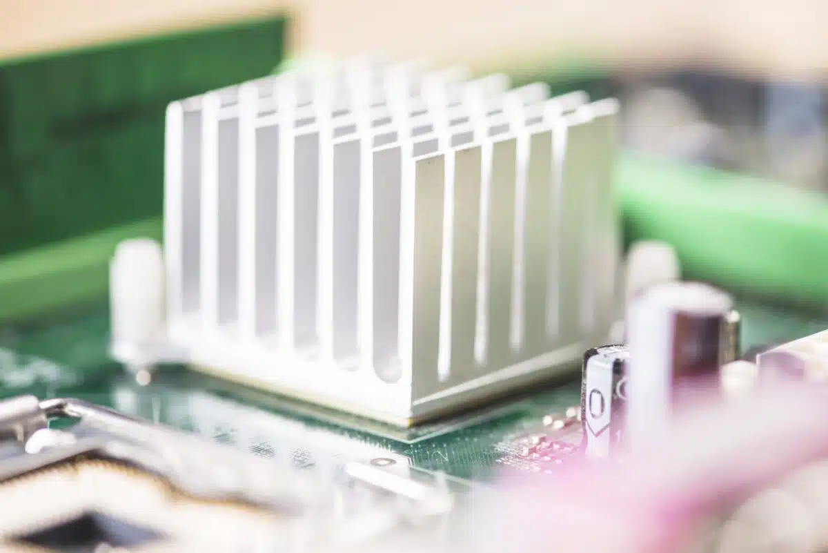
Temperature plays a governing role in DRAM refresh requirements because cell leakage increases exponentially with temperature, so retention time falls exponentially as the die heats up[5]. The dominant leakage paths at normal operating temperatures, subthreshold leakage through the access transistor and junction leakage at the storage node, are thermally activated with activation energies of roughly 0.5–0.7 eV, which is why their temperature dependence is commonly modeled with an Arrhenius relationship[3].

Across the normal operating range (case temperature up to 85°C, not just room temperature), DDR3 and DDR4 devices must have every cell refreshed within a 64 ms window, which the controller divides into 8,192 REFRESH commands issued an average of every 7.8 µs (tREFI)[1][2]. LPDDR4 uses a tighter 32 ms window, or one command roughly every 3.9 µs[10]. As operating conditions push into industrial ranges (commonly -40°C to +85°C, or to +95°C case temperature for many DDR4 parts) or automotive ranges (AEC-Q100 Grade 2 covers -40°C to +105°C and Grade 1 covers -40°C to +125°C ambient), cell retention time drops rapidly[1][14].

To prevent retention errors and bit corruption at high temperatures, dynamic memory specifications mandate refresh derating. For DDR4, once the DRAM case temperature (TC) exceeds 85°C the controller must double the refresh rate: the 64 ms refresh window shrinks to 32 ms and tREFI drops from about 7.8 µs to 3.9 µs[1][15]. Automotive-grade DDR4 extends this further, requiring a 16 ms window above 95°C and, for parts rated to 125°C, an 8 ms window above 105°C[1][4]. LPDDR4 handles derating through its on-die temperature sensor, which reports the required refresh rate in mode register MR4, from a 4x longer interval when cool down to a 0.25x interval when hot, and the controller must follow it[16].

Doubling the refresh rate has significant performance and power implications:

  • Power Escalation: The memory performs twice as many refresh operations, roughly doubling the refresh portion of memory power[1][2].
  • Reduced Availability: Each REFRESH command blocks access to the targeted banks for tRFC, so doubling the command rate doubles the time memory is unavailable, cutting throughput and adding latency jitter to time-critical tasks[2][17].
  • Added Heat: Extra refresh activity dissipates more power in the package, which can push die temperature higher in designs with marginal thermal paths. The increment is usually modest compared with active read/write power, but it compounds other thermal stresses in sealed enclosures.

When evaluating memory for sealed enclosures, outdoor gear, or densely packed boards, engineers must factor thermal derating directly into power estimates, using the refresh rates and IDD6 values specified at the highest expected case temperature. (Our Temperature Converter is handy when datasheets and environmental specs mix °C and °F.) Designing around nominal 25°C figures can badly understate field power: in one Micron LPDDR4X datasheet, the full-array self-refresh current listed for 85°C on the VDD2 rail is roughly nine times the 25°C value[6].

Temperature plays a governing role in DRAM refresh requirements because cell leakage increases exponentially with temperature, so retention time falls exponentially as the die heats up[5]. The dominant leakage paths at normal operating temperatures, subthreshold leakage through the access transistor and junction leakage at the storage node, are thermally activated with activation energies of roughly 0.5–0.7 eV, which is why their temperature dependence is commonly modeled with an Arrhenius relationship[3].

Across the normal operating range (case temperature up to 85°C, not just room temperature), DDR3 and DDR4 devices must have every cell refreshed within a 64 ms window, which the controller divides into 8,192 REFRESH commands issued an average of every 7.8 µs (tREFI)[1][2]. LPDDR4 uses a tighter 32 ms window, or one command roughly every 3.9 µs[10]. As operating conditions push into industrial ranges (commonly -40°C to +85°C, or to +95°C case temperature for many DDR4 parts) or automotive ranges (AEC-Q100 Grade 2 covers -40°C to +105°C and Grade 1 covers -40°C to +125°C ambient), cell retention time drops rapidly[1][14].

To prevent retention errors and bit corruption at high temperatures, dynamic memory specifications mandate refresh derating. For DDR4, once the DRAM case temperature (TC) exceeds 85°C the controller must double the refresh rate: the 64 ms refresh window shrinks to 32 ms and tREFI drops from about 7.8 µs to 3.9 µs[1][15]. Automotive-grade DDR4 extends this further, requiring a 16 ms window above 95°C and, for parts rated to 125°C, an 8 ms window above 105°C[1][4]. LPDDR4 handles derating through its on-die temperature sensor, which reports the required refresh rate in mode register MR4, from a 4x longer interval when cool down to a 0.25x interval when hot, and the controller must follow it[16].

Doubling the refresh rate has significant performance and power implications:

  • Power Escalation: The memory performs twice as many refresh operations, roughly doubling the refresh portion of memory power[1][2].
  • Reduced Availability: Each REFRESH command blocks access to the targeted banks for tRFC, so doubling the command rate doubles the time memory is unavailable, cutting throughput and adding latency jitter to time-critical tasks[2][17].
  • Added Heat: Extra refresh activity dissipates more power in the package, which can push die temperature higher in designs with marginal thermal paths. The increment is usually modest compared with active read/write power, but it compounds other thermal stresses in sealed enclosures.

When evaluating memory for sealed enclosures, outdoor gear, or densely packed boards, engineers must factor thermal derating directly into power estimates, using the refresh rates and IDD6 values specified at the highest expected case temperature. (Our Temperature Converter is handy when datasheets and environmental specs mix °C and °F.) Designing around nominal 25°C figures can badly understate field power: in one Micron LPDDR4X datasheet, the full-array self-refresh current listed for 85°C on the VDD2 rail is roughly nine times the 25°C value[6].

How Big Is the Power Overhead of DRAM Refresh in Battery-Powered Designs?
In battery-powered and duty-cycled systems, DRAM refresh can be one of the largest continuous drains on energy reserves, because mobile and embedded memory spends most of its time idle or operating at low data rates[12]. While active read and write commands consume higher instantaneous power, they only execute during short processing bursts. Refresh operations, conversely, run continuously to protect system memory, making refresh (IDD5B) and self-refresh (IDD6) current profiles critical parameters in overall system battery life calculations.

Refresh current during active operation is listed in DDR3, DDR4, and DDR5 datasheets as burst refresh current (IDD5B); DDR4 datasheets add IDD5F2 and IDD5F4 values for the fine granularity refresh modes, and LPDDR4 datasheets list auto-refresh currents including a per-bank value[8][10]. Each refresh opens one or more rows at once, and every open row drives thousands of bit lines through their sense amplifiers (rows typically hold 1–2 KB of data), producing short, repetitive current pulses[2]. In high-density chips like 8Gb or 16Gb DDR4 and LPDDR4, these pulses add to the transient load on the power distribution network, which is one more reason to place low equivalent series resistance (ESR) Capacitors close to the memory power pins for local decoupling.

When systems drop into deep sleep or standby mode, the metric shifts entirely to self-refresh current (IDD6). Although IDD6 is significantly lower in magnitude than active operational currents, its continuous nature over hours or days makes it a primary driver of the memory subsystem’s contribution to standby battery drain.

For a battery-powered device targeting extended field deployment, evaluating IDD6 currents across temperature variations is essential. As internal temperatures rise, IDD6 climbs steeply, both because leakage increases and because the device’s temperature sensor shortens the self-refresh interval. In one Micron DDR4 module datasheet, auto self-refresh current rises from 68.8 mA at 25°C to 248 mA at 75°C[3][15].

In battery-powered and duty-cycled systems, DRAM refresh can be one of the largest continuous drains on energy reserves, because mobile and embedded memory spends most of its time idle or operating at low data rates[12]. While active read and write commands consume higher instantaneous power, they only execute during short processing bursts. Refresh operations, conversely, run continuously to protect system memory, making refresh (IDD5B) and self-refresh (IDD6) current profiles critical parameters in overall system battery life calculations.

Refresh current during active operation is listed in DDR3, DDR4, and DDR5 datasheets as burst refresh current (IDD5B); DDR4 datasheets add IDD5F2 and IDD5F4 values for the fine granularity refresh modes, and LPDDR4 datasheets list auto-refresh currents including a per-bank value[8][10]. Each refresh opens one or more rows at once, and every open row drives thousands of bit lines through their sense amplifiers (rows typically hold 1–2 KB of data), producing short, repetitive current pulses[2]. In high-density chips like 8Gb or 16Gb DDR4 and LPDDR4, these pulses add to the transient load on the power distribution network, which is one more reason to place low equivalent series resistance (ESR) Capacitors close to the memory power pins for local decoupling.

When systems drop into deep sleep or standby mode, the metric shifts entirely to self-refresh current (IDD6). Although IDD6 is significantly lower in magnitude than active operational currents, its continuous nature over hours or days makes it a primary driver of the memory subsystem’s contribution to standby battery drain.

For a battery-powered device targeting extended field deployment, evaluating IDD6 currents across temperature variations is essential. As internal temperatures rise, IDD6 climbs steeply, both because leakage increases and because the device’s temperature sensor shortens the self-refresh interval. In one Micron DDR4 module datasheet, auto self-refresh current rises from 68.8 mA at 25°C to 248 mA at 75°C[3][15].

What System-Level Mitigations Reduce DRAM Refresh Power?

To minimize the power impact of mandatory refresh commands, system architects can implement hardware and firmware-level mitigations. These techniques optimize how and when refresh cycles run, ensuring data retention without unnecessarily straining battery budgets.

Key mitigation strategies include:

Temperature-Compensated Self-Refresh (TCSR)

Modern low-power DRAM ICs feature built-in temperature sensors that dynamically adjust internal self-refresh rates[6][10]. Rather than running the self-refresh oscillator at a fixed, worst-case high-temperature rate, TCSR automatically lengthens the refresh interval when the die is cool, significantly lowering IDD6 current draw at ambient temperatures[12]. Standard DDR4 offers a comparable option called Low-Power Auto Self Refresh (LPASR)[1][11].

Partial-Array Self-Refresh (PASR) Configuration

Firmware developers can structure system software to consolidate persistent data into designated memory banks. By writing the DRAM’s PASR mode registers before entering sleep (in LPDDR2 and later, MR16 masks individual banks and MR17 masks segments), firmware removes non-essential regions from self-refresh, directly reducing standby current draw. Data in masked regions is not retained[7][10].

Fine Granularity Refresh (FGR) and Per-Bank Refresh

In DDR3 and DDR4, each REFRESH command occupies every bank on the rank for tRFC[2]. DDR4 Fine Granularity Refresh (FGR) issues refresh commands two or four times as often (0.5x or 0.25x tREFI), with each command refreshing fewer rows, so the rank is blocked for a shorter tRFC per command, though not proportionally shorter[18]. This reduces worst-case access latency, but it doesn’t reduce the total refresh work. Per-bank refresh (called directed per-bank refresh in LPDDR4 and Same Bank Refresh in DDR5) lets the controller refresh some banks while others continue serving reads and writes, improving memory availability[6][17][19].

Controller-Level Scheduling

DDR memory controllers in application processors, and in higher-end Microcontrollers with an external DDR interface, can use the JEDEC allowance to postpone or pull in up to eight refresh commands, shifting refresh into brief idle windows based on bus activity[2]. This minimizes latency impact on burst memory accesses, but it doesn’t reduce the total number of refreshes, so refresh energy stays essentially the same[2].

How Should Refresh Overhead Influence Your Memory Selection?

Addressing DRAM refresh overhead requires assessing trade-offs during initial component selection rather than attempting firmware workarounds late in product development. Matching memory technology to application power requirements prevents late-stage board redesigns and unexpected power budget breaches.

For ultra-low-power edge nodes or duty-cycled equipment, specialty low-power memory lines, such as the LPDDR devices from Jeju Semiconductor (JSC), include PASR and auto TCSR to minimize idle current draw[20]. Conversely, if high operating temperatures are expected, select industrial- or automotive-grade memory rated for the expected case temperature, and build the refresh derating from its datasheet into the power model[1][4].

Use this structural design checklist when evaluating dynamic memory for power-sensitive or thermally challenging applications:

Verify Controller Capabilities

Ensure the host memory controller or processor supports features like TCSR, PASR, and Per-Bank Refresh scheduling.

Analyze Decoupling & PDN Limits

Check power distribution network designs to ensure local ceramic decoupling capacitors can absorb transient current spikes during active refresh (IDD5B).

Evaluate Alternative Technologies

If self-refresh power targets cannot be met with standard DRAM, evaluate pseudo-SRAM (pSRAM), which uses DRAM cells with fully internal refresh behind an SRAM-style interface and is typically offered at lower densities, or ultra-low-power LPDDR4x Memory architectures tailored for low standby drain[21].

Calculate IDD6 Baseline

Estimate standby power consumption based on high-temperature self-refresh current (IDD6) rather than room-temperature nominal specs[6][15].

Partition Memory Architecture

Verify that software/firmware can segregate critical retention data into specific memory banks to leverage PASR masking during extended system sleep.

Define Thermal Operating Limits

Identify the maximum DRAM case temperature (TC) under worst-case ambient conditions to determine whether refresh derating will be triggered (2x refresh, a 32 ms window, above 85°C for DDR4; 4x refresh, a 16 ms window, above 95°C for automotive-grade parts)[1][4].

For complex design requirements, engaging early with specialized technical resources simplifies part selection. Suntsu’s Component Engineering Support team assists design groups in navigating memory trade-offs, evaluating thermal datasheets, and identifying optimal memory IC types for challenging operational environments.

Optimizing Memory Power with Suntsu

Managing DRAM refresh overhead requires balancing operational temperature limits, standby power targets, and memory controller capabilities. By factoring refresh (IDD5B) and self-refresh (IDD6) currents into early power budget models, engineering teams avoid unexpected thermal issues and battery life shortfalls in production.

Suntsu provides comprehensive technical support to help hardware teams select and integrate power-optimized memory components. Through specialized Engineering Design Support and global sourcing capabilities for leading Memory ICs, Suntsu helps engineers overcome complex power and thermal challenges.

Worked through the checklist and know what your design needs? Share your thermal limits, standby current targets, and controller requirements, and our team can help.

FAQs

DDR5 tightens the base refresh window to 32 ms (tREFI of about 3.9 µs) at normal temperatures, half of DDR4’s 64 ms. To offset the extra refresh work, DDR5 adds Same Bank Refresh, which refreshes the same bank across every bank group while the other banks keep serving traffic. Above 85°C, the interval halves again.

Deep Power-Down (DPD) switches off the memory array’s internal power almost entirely. Standby current drops below self-refresh levels, but every bit of stored data is lost. It suits systems that can reload their contents from flash on wake-up and can accept the longer restart time. Not every DRAM generation supports it; LPDDR4, for example, dropped DPD.

Rowhammer is a disturbance effect: repeatedly activating one row can leak charge from cells in adjacent rows and flip bits before their next scheduled refresh. Refresh is part of the defense. Some systems increase refresh rates to shrink the attack window, DDR4 devices use Target Row Refresh (TRR), and DDR5 and LPDDR5 add Refresh Management (RFM) commands. All of these mitigations add some refresh overhead.

ECC corrects occasional bit errors, including a weak cell that loses charge early, so it improves reliability. DDR5 also includes on-die ECC. However, standard controllers still refresh at the full JEDEC rate. Academic proposals that combine ECC with retention profiling to stretch refresh intervals haven’t become standard practice.

Not safely in production hardware. Refresh intervals are set to protect the weakest cells in the device across temperature and voltage. Those cells vary from part to part and can change over time, an effect known as variable retention time. Running below spec voids the manufacturer’s data retention guarantee. If you need lower standby power, the supported tools are PASR, TCSR, and a different memory choice.

References

  1. Micron Technology. “8Gb: x4, x8, x16 DDR4 SDRAM Datasheet” Available at: https://www.mouser.com/datasheet/2/671/Micron_05092023_8gb_ddr4_sdram-3175546.pdf
  2. J. Liu, B. Jaiyen, R. Veras, and O. Mutlu. “RAIDR: Retention-Aware Intelligent DRAM Refresh” Available at: https://users.ece.cmu.edu/~omutlu/pub/raidr-dram-refresh_isca12.pdf
  3. H.-J. Kim, W.-C. Lee, and H.-J. Park. “RAIDR: Retention-Aware Intelligent DRAM Refresh” Available at: http://journal.auric.kr/AURIC_OPEN_temp/RDOC/ieie02/ieiejsts_202206_001.pdf
  4. Micron Technology. “16Gb Automotive DDR4 SDRAM (Z42B) datasheet” Available at: https://mm.digikey.com/Volume0/opasdata/d220001/medias/docus/8827/557_16gb-auto-ddr4-z42b.pdf
  5. J. Meza. “Large Scale Studies of Memory, Storage, and Network Failures in a Modern Data Center” Available at: https://arxiv.org/pdf/1901.03401
  6. Micron Technology. “LPDDR4/LPDDR4X SDRAM Embedded Datasheet” Available at: https://www.mouser.com/datasheet/2/671/z3bm_embedded_lpddr4_lpddr4x-3193457.pdf
  7. M. Coquelin. “[RFCv1 0/6] PASR: Partial Array Self-Refresh Framework” Available at: https://lkml.iu.edu/hypermail/linux/kernel/1201.3/02586.html
  8. Advantech. “SQRAM DDR4-2400 16GB UDIMM Datasheet” Available at: https://advdownload.advantech.com/productfile/Downloadfile4/1-26XPP59/ADVANTECH_SQR-UD4N16G2K4HNHAC.pdf
  9. K. Kim and J. Lee. “A New Investigation of Data Retention Time in Truly Nanoscaled DRAMs” Available at: https://www.researchgate.net/publication/224562908_A_New_Investigation_of_Data_Retention_Time_in_Truly_Nanoscaled_DRAMs
  10. Kingston Technology. “Low Power DRAM (LPDDR4 FBGA) Datasheet” Available at: https://www.mouser.com/catalog/specsheets/Kingston_01-31-2025_KTC_LPDDR4_200Ball_D1611PM3BDGUI-U_VerD.pdf
  11. D. Chinnakkonda, V.-K. Tavva, and M.B,. Srinivas. “Voltage Reduced Self Refresh (VRSR) for optimized energy savings in DRAM Memories” Available at: https://www.sciencedirect.com/science/article/pii/S277306462300035X
  12. Winbond Electronics. “Combining deep power-down with self-refresh mode” Available at: https://www.winbond.com/hq/support/online-learning/articles-item/combining-deep-power-down-with-self-refresh-mode.html?__locale=en
  13. Micron Technology. “Automotive LPDDR4/LPDDR4X SDRAM Datasheet” Available at: https://www.mouser.com/datasheet/2/671/200b_z32m_sdp_ddp_qdp_auto_lpddr4_lpddr4x-3165056.pdf
  14. Automotive Electronics Council. “AEC-Q100 Rev-J: Failure Mechanism Based Stress Test Qualification for Integrated Circuits” Available at: http://www.aecouncil.com/Documents/AEC_Q100_Rev_J_Base_Document.pdf
  15. Micron Technology. “DDR4 SDRAM SODIMM MTA8ATF1G64HZ Datasheet” Available at: https://media.digikey.com/pdf/Data Sheets/Micron Technology Inc PDFs/MTA8ATF1G64HZ_8GB_DS.pdf
  16. Integrated Silicon Solution Inc. (ISSI). “IS43/46LQ16512B LPDDR4 Datasheet” Available at: https://www.mouser.com/catalog/specsheets/Integrated-Silicon-Solution_11-12-2024_43-46LQ16512B.pdf
  17. Micron Technology. “Micron DDR5 SDRAM: New Features” Available at: https://assets.micron.com/adobe/assets/urn:aaid:aem:5ea148c8-e3fe-489e-8489-99b1b9cdcd3c/renditions/original/as/ddr5-new-features-white-paper.pdf
  18. J. Mukundan, H. Hunter, K.-H. Kim, J. Stuecheli, and J. F. Martínez. “Understanding and Mitigating Refresh Overheads in High-Density DDR4 DRAM Systems” Available at: https://people.ece.cornell.edu/martinez/doc/isca13-mukundan.pdf
  19. SK hynix Newsroom. “Why DDR5 is the Industry’s Powerful Next-gen Memory?” Available at: https://news.skhynix.com/why-ddr5-is-the-industrys-powerful-next-gen-memory/
  20. Jeju Semiconductor Corp. (JSC). “Low Power DRAM” Available at: http://www.jeju-semi.com/Products/LPDRAM
  21. Silicon Labs. “Pseudo-Static Random Access Memory (PSRAM) Developer Guide” Available at: https://docs.silabs.com/wiseconnect/latest/external-memory-psram//

keyboard_arrow_up