
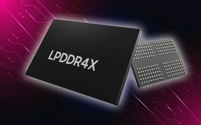
16Gb LPDDR4x Memory Allocation: JSC JSL4BAG167ZAMF-05A

When designing high-performance embedded systems, industrial platforms, or advanced portable devices, choosing the right volatile memory means balancing power efficiency against data throughput. System architects also face a second problem that has nothing to do with silicon: securing a reliable allocation without compromising on the part they specified. To help teams work around those supply constraints, Suntsu Electronics offers a dedicated allocation of LPDDR4x memory from Jeju Semiconductor Corporation (JSC), led by the 16Gb single-channel device, part number JSL4BAG167ZAMF-05A.

JSC is a Korean fabless memory supplier that concentrates on low-power, low-density devices for IoT, mobile, networking, and automotive electronics[8]. The JSL4BAG167ZAMF family also appears on NXP’s i.MX 93 memory compatibility list as a validated 16Gb (2GB) LPDDR4x option[7], so the part has documented design-in history on a mainstream applications processor rather than being an unfamiliar substitution.

Understanding the structural setup, interface functions, and architectural benefits of this component helps design and procurement teams optimize system efficiency. Assessing these technical details facilitates easier integration and reduces the risk of long-term obsolescence or shortages.

When designing high-performance embedded systems, industrial platforms, or advanced portable devices, choosing the right volatile memory means balancing power efficiency against data throughput. System architects also face a second problem that has nothing to do with silicon: securing a reliable allocation without compromising on the part they specified. To help teams work around those supply constraints, Suntsu Electronics offers a dedicated allocation of LPDDR4x memory from Jeju Semiconductor Corporation (JSC), led by the 16Gb single-channel device, part number JSL4BAG167ZAMF-05A.

JSC is a Korean fabless memory supplier that concentrates on low-power, low-density devices for IoT, mobile, networking, and automotive electronics[8]. The JSL4BAG167ZAMF family also appears on NXP’s i.MX 93 memory compatibility list as a validated 16Gb (2GB) LPDDR4x option[7], so the part has documented design-in history on a mainstream applications processor rather than being an unfamiliar substitution.

Understanding the structural setup, interface functions, and architectural benefits of this component helps design and procurement teams optimize system efficiency. Assessing these technical details facilitates easier integration and reduces the risk of long-term obsolescence or shortages.

Key Takeaways

  • Reduced I/O Voltage: LPDDR4x drops VDDQ from the 1.1V used by LPDDR4 to 0.6V, a roughly 40% reduction in I/O supply voltage that JEDEC identifies as the defining change in the LPDDR4X addendum[1]. Core rails stay at VDD1 1.8V and VDD2 1.1V[4].
  • Data rate: The –05A speed grade is rated to 4266 Mbps (2133 MHz clock); the –05 grade runs 3733 Mbps[8].
  • Single channel, dual rank: Organized as one x16 channel with two ranks and 8 internal banks per channel[4]. The host controller must explicitly support dual-rank single-channel operation.
  • Industrial temperature rating: Tc = –40°C to +95°C. This is an industrial range, not an AEC-Q100 automotive grade[6].
  • Allocation support: Suntsu provides direct access to allocation availability and engineering samples for upcoming production builds.
Secure Your Component Allocation

Don’t let memory component shortages stall your production timeline. Suntsu Electronics maintains dedicated allocation access for the JSC 16Gb LPDDR4x (JSL4BAG167ZAMF-05A) memory solution, ensuring your next build stays on schedule.

Secure Your Component Allocation

Don’t let memory component shortages stall your production timeline. Suntsu Electronics maintains dedicated allocation access for the JSC 16Gb LPDDR4x (JSL4BAG167ZAMF-05A) memory solution, ensuring your next build stays on schedule.

What Is the Primary Advantage of LPDDR4x Over Standard LPDDR4?
Low-Power Double Data Rate 4X is an optional extension to the LPDDR4 standard rather than a new generation. JEDEC published it as Addendum No. 1 to JESD209-4 alongside JESD209-4B in 2017[2]. The headline change is the input/output supply voltage: where LPDDR4 uses a VDDQ of 1.1V, LPDDR4x reduces it to 0.6V while leaving the core rails at VDD1 1.8V and VDD2 1.1V[1][4].

Because I/O driver power scales with supply voltage, cutting VDDQ reduces the energy spent moving data across the bus, on both the memory and the controller side of the link. The same generation of changes also raised the maximum data rate from 3200 Mbps on LPDDR4 to 4266 Mbps by adding termination and calibration options[10]. For battery-powered devices and thermally constrained embedded systems, that combination of lower I/O power and higher peak bandwidth is the reason LPDDR4x displaced LPDDR4 in most new designs. One practical caveat: LPDDR4x is not backward compatible with LPDDR4, and LPDDR4x parts are not required to

tolerate the higher LPDDR4 I/O voltage[10].

Engineers comparing alternatives can review the broader DRAM memory range to match a device to specific system requirements, and the wider Integrated Circuits catalog for adjacent parts. Note that the LPDDR4x clock is generated by the SoC memory controller PHY rather than by a discrete timing device, so an external oscillator or other frequency control device serves the system reference clock, not the memory interface itself — a distinction covered in our Quick Guide to Oscillators.

Low-Power Double Data Rate 4X is an optional extension to the LPDDR4 standard rather than a new generation. JEDEC published it as Addendum No. 1 to JESD209-4 alongside JESD209-4B in 2017[2]. The headline change is the input/output supply voltage: where LPDDR4 uses a VDDQ of 1.1V, LPDDR4x reduces it to 0.6V while leaving the core rails at VDD1 1.8V and VDD2 1.1V[1][4].

Because I/O driver power scales with supply voltage, cutting VDDQ reduces the energy spent moving data across the bus, on both the memory and the controller side of the link. The same generation of changes also raised the maximum data rate from 3200 Mbps on LPDDR4 to 4266 Mbps by adding termination and calibration options[10]. For battery-powered devices and thermally constrained embedded systems, that combination of lower I/O power and higher peak bandwidth is the reason LPDDR4x displaced LPDDR4 in most new designs. One practical caveat: LPDDR4x is not backward compatible with LPDDR4, and LPDDR4x parts are not required to tolerate the higher LPDDR4 I/O voltage[10].

Engineers comparing alternatives can review the broader DRAM memory range to match a device to specific system requirements, and the wider Integrated Circuits catalog for adjacent parts. Note that the LPDDR4x clock is generated by the SoC memory controller PHY rather than by a discrete timing device, so an external oscillator or other frequency control device serves the system reference clock, not the memory interface itself — a distinction covered in our Quick Guide to Oscillators.

Thermal Behaviour and Temperature Grade
Thermal dissipation remains a hard physical limit in compact electronic packaging. As processor speeds rise and peripheral integration expands, heat concentrates locally and can lead to throttling or accelerated wear. Lower I/O voltage helps here directly: less energy per bit transferred means less heat generated in the driver stages at a given data rate.

The JSL4BAG167ZAMF-05A is specified over an operating case temperature (Tc) range of –40°C to +95°C. That is an industrial rating. It is worth stating

plainly, because it is easy to conflate a wide temperature range with automotive qualification: AEC-Q100, the automotive stress-test standard, defines its grades by ambient temperature, with Grade 2 at –40°C to +105°C and Grade 1 at –40°C to +125°C[6]. A –40°C to +95°C case rating does not meet either threshold. Teams targeting automotive programs should request AEC-Q100 qualification documentation for a specific automotive-designated part number rather than inferring it from the temperature range.

For industrial and outdoor enclosures, the range is genuinely useful. LPDDR4x devices also integrate an on-die temperature sensor, readable through the mode registers, that lets the memory controller raise the self-refresh rate as the die heats up and apply timing derating where required[4][9]. Designers should confirm their controller actually implements that temperature-tracking behavior, since retention margin at the top of the range depends on it. For context on how market conditions affect sourcing for high-density assemblies, see Build a Component Procurement Strategy That Survives a Shortage.

Thermal dissipation remains a hard physical limit in compact electronic packaging. As processor speeds rise and peripheral integration expands, heat concentrates locally and can lead to throttling or accelerated wear. Lower I/O voltage helps here directly: less energy per bit transferred means less heat generated in the driver stages at a given data rate.

The JSL4BAG167ZAMF-05A is specified over an operating case temperature (Tc) range of –40°C to +95°C. That is an industrial rating. It is worth stating plainly, because it is easy to conflate a wide temperature range with automotive qualification: AEC-Q100, the automotive stress-test standard, defines its grades by ambient temperature, with Grade 2 at –40°C to +105°C and Grade 1 at –40°C to +125°C[6]. A –40°C to +95°C case rating does not meet either threshold. Teams targeting automotive programs should request AEC-Q100 qualification documentation for a specific automotive-designated part number rather than inferring it from the temperature range.

For industrial and outdoor enclosures, the range is genuinely useful. LPDDR4x devices also integrate an on-die temperature sensor, readable through the mode registers, that lets the memory controller raise the self-refresh rate as the die heats up and apply timing derating where required[4][9]. Designers should confirm their controller actually implements that temperature-tracking behavior, since retention margin at the top of the range depends on it. For context on how market conditions affect sourcing for high-density assemblies, see Build a Component Procurement Strategy That Survives a Shortage.

Architectural Configuration and Density of the JSC 16Gb LPDDR4x

The JSL4BAG167ZAMF-05A carries a well-defined set of physical and logical attributes suited to dense embedded designs. The table below summarizes the configuration.

ParameterSpecification
Part NumberJSL4BAG167ZAMF-05A
ManufacturerJeju Semiconductor Corporation (JSC)
Density16Gb (2GB)
OrganizationSingle channel, dual rank (1ch x16, 2 ranks)
Banks8 internal banks per channel
Package200-ball FBGA, 10.0 x 15.0 x 1.0 mm (max)
Operating TemperatureTc = –40°C to +95°C (industrial)
Max Data Rate4266 Mbps / 2133 MHz (–05A grade); 3733 Mbps (–05 grade)
I/O SignalingLVSTL with VSSQ termination
Supply RailsVDD1 1.8V, VDD2 1.1V, VDDQ 0.6V

The dual-rank arrangement is the detail most likely to affect integration. A dual-rank single-channel device presents two chip-select and two clock-enable signals on the same x16 channel[4], so both the board routing and the memory controller configuration have to account for the second rank. NXP documents dual-rank single-channel support explicitly as one route to 16Gb density on the i.MX 93[7]. A design set up for a single-rank 16Gb part will not simply drop this device in.

The 200-ball FBGA in a 10.0 x 15.0 mm footprint is the standard package for this density class, which is helpful for second-sourcing: it is the same outline used by comparable LPDDR4x devices from other suppliers [4][9]. For selection methodology, see our guide on Memory IC Essentials, and for background on memory types, What is DRAM and How Do I Pick the Correct Type?.

What Purpose Does Data Bus Inversion (DBI) Serve?

The JSL4BAG167ZAMF-05A supports Data Bus Inversion, signaled on the DMI (Data Mask Inversion) pins and enabled separately for reads and writes through mode register 3[4].

Why it matters comes down to the signaling scheme. LPDDR4 and LPDDR4x use LVSTL (Low Voltage Swing Terminated Logic) with termination to VSSQ, an arrangement that draws no termination current while a line sits low. Fewer logic ones on the bus therefore means less I/O power[3]. DBI

exploits that at byte granularity: when more than four of the eight bits in a byte would be driven high, the transmitter inverts the entire byte and drives the corresponding DMI pin high so the receiver knows to invert it back[3].

The primary benefit is reduced I/O termination power rather than reduced switching power. Capping the number of simultaneously driven-high lines does also limit simultaneous switching noise across the byte lane, which helps signal integrity at 4266 Mbps, but power is the main motivation. When DBI is turned off, the same DMI pin reverts to its data mask (DM) role for masked writes[4] — the two functions share the pin and are selected by mode register setting, so a controller cannot use both simultaneously on the same operation. Broader context on these devices is available in our Semiconductor Components overview.

The JSL4BAG167ZAMF-05A supports Data Bus Inversion, signaled on the DMI (Data Mask Inversion) pins and enabled separately for reads and writes through mode register 3[4].

Why it matters comes down to the signaling scheme. LPDDR4 and LPDDR4x use LVSTL (Low Voltage Swing Terminated Logic) with termination to VSSQ, an arrangement that draws no termination current while a line sits low. Fewer logic ones on the bus therefore means less I/O power[3]. DBI exploits that at byte granularity: when more than four of the eight bits in a byte would be driven high, the transmitter inverts the entire byte and drives the corresponding DMI pin high so the receiver knows to invert it back[3].

The primary benefit is reduced I/O termination power rather than reduced switching power. Capping the number of simultaneously driven-high lines does also limit simultaneous switching noise across the byte lane, which helps signal integrity at 4266 Mbps, but power is the main motivation. When DBI is turned off, the same DMI pin reverts to its data mask (DM) role for masked writes[4] — the two functions share the pin and are selected by mode register setting, so a controller cannot use both simultaneously on the same operation. Broader context on these devices is available in our Semiconductor Components overview.

Does LPDDR4x Utilize a DLL (Delay-Locked Loop)?

No. Engineers moving from desktop or server DDR memory often expect one, since DDR SDRAM devices include an on-die DLL to align internal clocking with the external system clock. LPDDR4x devices, including this JSC part, omit the DLL entirely; the published feature set for this class of device states it directly as “no DLL: CK to DQS is not synchronized”[4].

Removing the DLL saves power and die area, but it shifts the timing burden onto the memory controller. The device presents an open-loop output path: read data is edge-aligned to DQS, and write data must be centered on DQS by the controller[4]. To close that gap, LPDDR4x relies on a training sequence run at initialization — write leveling, command bus and CA training, internal VREF training, and FIFO-based read/write training[3][4] — which measures and compensates for propagation delay and phase mismatch on the actual board. In practice this means the PHY and its training routines matter as much as the DRAM itself, and it is why a part that trains successfully on one platform may need retuning on another.

Board Layout Constraints and Signal Integrity
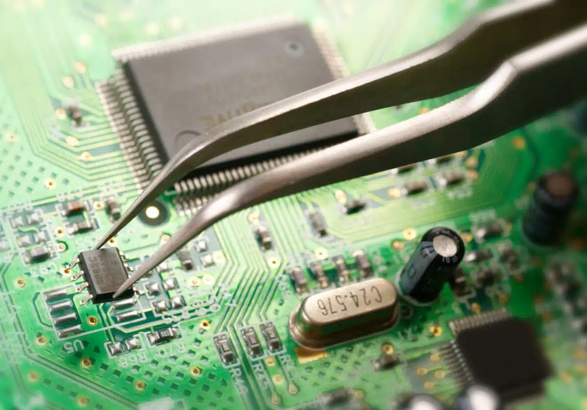
Routing a 4266 Mbps memory interface demands tight control of trace length matching, impedance, and layer stackup, because small impedance discontinuities produce reflections and timing jitter that eat directly into the training margin described above.

Target impedances should come from the SoC vendor’s guide for the specific PHY, not from generic DDR practice. AMD’s Versal PCB design guide, for example, specifies 45 Ω ±10% single-ended for command/address/control and data signals, and 82 Ω ±10% differential for

clock and data strobe pairs on LPDDR4/4x[5]. Other silicon vendors commonly call for roughly 40 Ω single-ended and about 80 Ω differential. The 50 Ω / 100 Ω pairing familiar from general-purpose high-speed digital design is not the right target for this interface.

Beyond impedance, place decoupling capacitors immediately adjacent to the VDD1, VDD2, and VDDQ power balls to suppress high-frequency transient noise, and keep ground reference planes continuous beneath the 200-ball FBGA so high-speed signals have an uninterrupted return path. AMD’s guide also constrains via count and inter-signal spacing in multiples of the dielectric height[5], which is worth reviewing before committing a stackup. The All Products catalog covers the passives and timing devices these designs require. For market context, see Navigating the 2026 Memory and NAND Flash Price Surge.

Routing a 4266 Mbps memory interface demands tight control of trace length matching, impedance, and layer stackup, because small impedance discontinuities produce reflections and timing jitter that eat directly into the training margin described above.

Target impedances should come from the SoC vendor’s guide for the specific PHY, not from generic DDR practice. AMD’s Versal PCB design guide, for example, specifies 45 Ω ±10% single-ended for command/address/control and data signals, and 82 Ω ±10% differential for clock and data strobe pairs on LPDDR4/4x[5]. Other silicon vendors commonly call for roughly 40 Ω single-ended and about 80 Ω differential. The 50 Ω / 100 Ω pairing familiar from general-purpose high-speed digital design is not the right target for this interface.

Beyond impedance, place decoupling capacitors immediately adjacent to the VDD1, VDD2, and VDDQ power balls to suppress high-frequency transient noise, and keep ground reference planes continuous beneath the 200-ball FBGA so high-speed signals have an uninterrupted return path. AMD’s guide also constrains via count and inter-signal spacing in multiples of the dielectric height[5], which is worth reviewing before committing a stackup. The All Products catalog covers the passives and timing devices these designs require. For market context, see Navigating the 2026 Memory and NAND Flash Price Surge.

Securing Your Supply Chain

Sourcing dependable memory ICs in a volatile market depends on trusted distribution relationships. Alongside memory devices, continuous manufacturing requires a steady flow of specialized parts and passive components. Suntsu Electronics uses its industry relationships to secure allocations for constrained components and keep production lines moving.

Don’t let supply chain volatility disrupt your next production run. Suntsu Electronics has secured dedicated allocation access for the JSC 16Gb LPDDR4x (JSL4BAG167ZAMF-05A) memory solution. Contact us today to request engineering samples, check current pricing, and secure your allocation inventory.

FAQs

LPDDR4x reduces the input/output power supply voltage (VDDQ) from 1.1V down to 0.6V while maintaining the same core voltage rails, which significantly decreases active power dissipation and thermal output in compact or battery-operated devices.

LPDDR4x omits the internal Delay-Locked Loop to conserve power, utilizing an open-loop architecture where data outputs are edge-aligned by design and managed via initialization training routines.

Data Bus Inversion evaluates the logic state of a data payload and inverts the bus if more than half of the bits are high, reducing simultaneous switching noise and lowering dynamic power consumption during read and write operations.

The Data Mask Inversion (DMI) pins manage data bus inversion status indicators and support data masking functions during write operations.

No, memory controllers must natively support the lower 0.6V VDDQ voltage interface level (LVSTL_06) and specific command training protocols required by LPDDR4x specifications.

References

  1. JEDEC. “Low Power Memory: LPDDR” Available at: https://www.jedec.org/category/technology-focus-area/mobile-memory-lpddr-wide-io-memory-mcp
  2. JEDEC. “JEDEC Updates Standards for Low Power Memory Devices” Available at: https://www.jedec.org/news/pressreleases/jedec-updates-standards-low-power-memory-devices-0
  3. Synopsys. “Maximizing Mobile Performance with LPDDR4 SoC RAM” Available at: https://www.synopsys.com/blogs/chip-design/maximizing-mobile-performance-lpddr4-ram.html
  4. Alliance Memory. “8Gb/16Gb/32Gb LPDDR4X SDRAM datasheet” Available at: https://www.mouser.com/datasheet/3/893/1/AllianceMemory_8Gb_16Gb_32Gb_LPDDR4X_AS4C512M16MD4V_AS4C1G16MD4V_AS4C512.pdf
  5. AMD. “Physical Design Rules for LPDDR4/4x Signals” Available at: https://docs.amd.com/r/en-US/ug863-versal-pcb-design/Physical-Design-Rules-for-LPDDR4/4x-Signals
  6. Automotive Electronics Council. “Definition of Part Operating Temperature Grade” Available at: http://www.aecouncil.com/Documents/AEC_Q100_Rev_F2.pdf
  7. NXP. “i.MX 93 Memory Compatibility Guide” Available at: https://community.nxp.com/t5/i-MX-Processors-Knowledge-Base/i-MX-93-Memory-Compatibility-Guide/ta-p/1725656
  8. Jeju Semiconductor Corporation (JSC). “Low Power DRAM Products” Available at: http://www.jeju-semi.com/Products/LPDRAM
  9. Micron. “LPDDR4X/LPDDR4 SDRAM datasheet” Available at: https://mm.digikey.com/Volume0/opasdata/d220001/medias/docus/8606/z42m-embedded-lpddr4x-lpddr4.pdf
  10. FuturePlus Systems. “LPDDR4 to LPDDR4X: What is the difference?” Available at: https://www.futureplus.com/blog/lpddr4-to-lpddr4x-what-is-the-difference

keyboard_arrow_up