
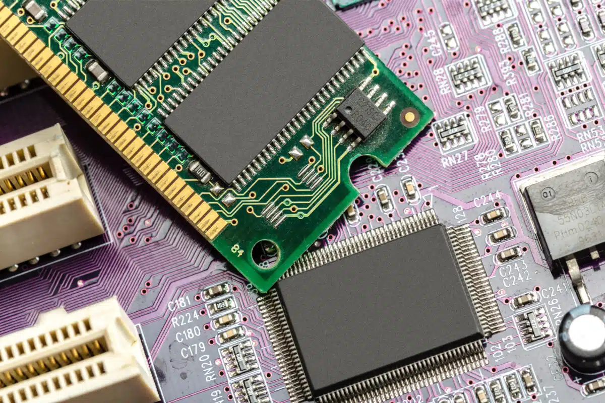
Parameter Specification Part Number H5TQ4G83EFR-TEI Density/Organization 4 Gb — 512M × 8 (512 MB) Speed Grade -TE — DDR3-2133, CL 14-14-14 Temperature Grade I — Industrial, −40 °C to +95 °C Package 78-ball FBGA, 7.5 × 11.0 mm Supply Rail 1.5 V standard DDR3
Why Legacy Architecture Persists
A common question in product lifecycle planning is why hardware programs often still use and procure DDR3 Memory instead of switching directly to newer standards like DDR4 or DDR5. The explanation typically involves factors such as system cost, the maturity of the architecture, long-term lifecycle economics, and how well the memory fits the computational requirements.
1. Embedded SoC and Controller Native Compatibility
2. Streamlined PCB Layout and Lower Layer Counts
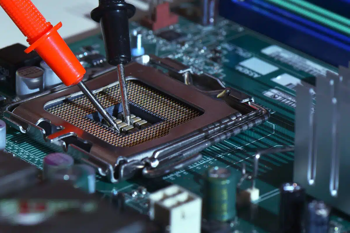
Implementing advanced high-speed memory demands complex signal integrity techniques, tighter length matching, and increased layer counts to manage impedance and cross-talk. Standard DDR3 operates at moderate transfer rates—such as DDR3-1333, DDR3-1600, DDR3-1866, and DDR3-2133—which allow for reliable routing on stackups with fewer layers compared to equivalent DDR4 or DDR5 setups. Our Engineering Design Services often reveal that using mature memory buses helps maintain target price points in high-volume assemblies.
3. Regulatory and Certification Lock-In
In industries like aerospace, medical diagnostics, energy infrastructure, and industrial automation, the obsolescence of a core component impacts more than just purchasing. For medical devices, replacing a critical part involves documented risk and performance assessments, along with potential notification and re-certification with the FDA—such as revisiting existing 510(k) or PMA submissions—and conducting third-party EMI/EMC testing, packaging evaluations, and comprehensive verification and validation processes[11]. The real costs often stem from redesigning, testing, regulatory reviews, and managing supply gaps during qualification. Securing guaranteed allocations of proven DDR3 memory safeguards established platforms from early EOL, postponing the entire process. For a broader view on market fluctuations affecting DRAM, see our analysis on DDR4 Market Volatility: How Independent Distributors Ensure Project Continuity.
Technical Analysis: Standard DDR3 vs. DDR3L
Understanding the operating envelope of memory is essential for designing power distribution networks (PDNs) and managing thermal performance. A key technical factor in choosing components is differentiating between the standard DDR3 and its lower-voltage version, DDR3L.
Specification Parameter Standard DDR3 Low-Voltage DDR3L Nominal Supply Voltage (VDD/VDDQ) 1.5V ± 0.075V 1.35V (1.283V to 1.45V) Backward Compatibility Operates strictly at 1.5V Interoperable at both 1.35V and 1.5V rails I/O Logic Signaling SSTL_15 SSTL_135 System Application Fit Line-powered industrial gear, fixed infrastructure, legacy boards Battery-backed systems, low-power edge compute, mobile devices Noise Immunity Margin Wider voltage swings provide robust noise margins in harsh EMI Optimized for energy conservation with lower power dissipation
Deep Dive: SK Hynix 4Gb DDR3 SDRAM Architecture
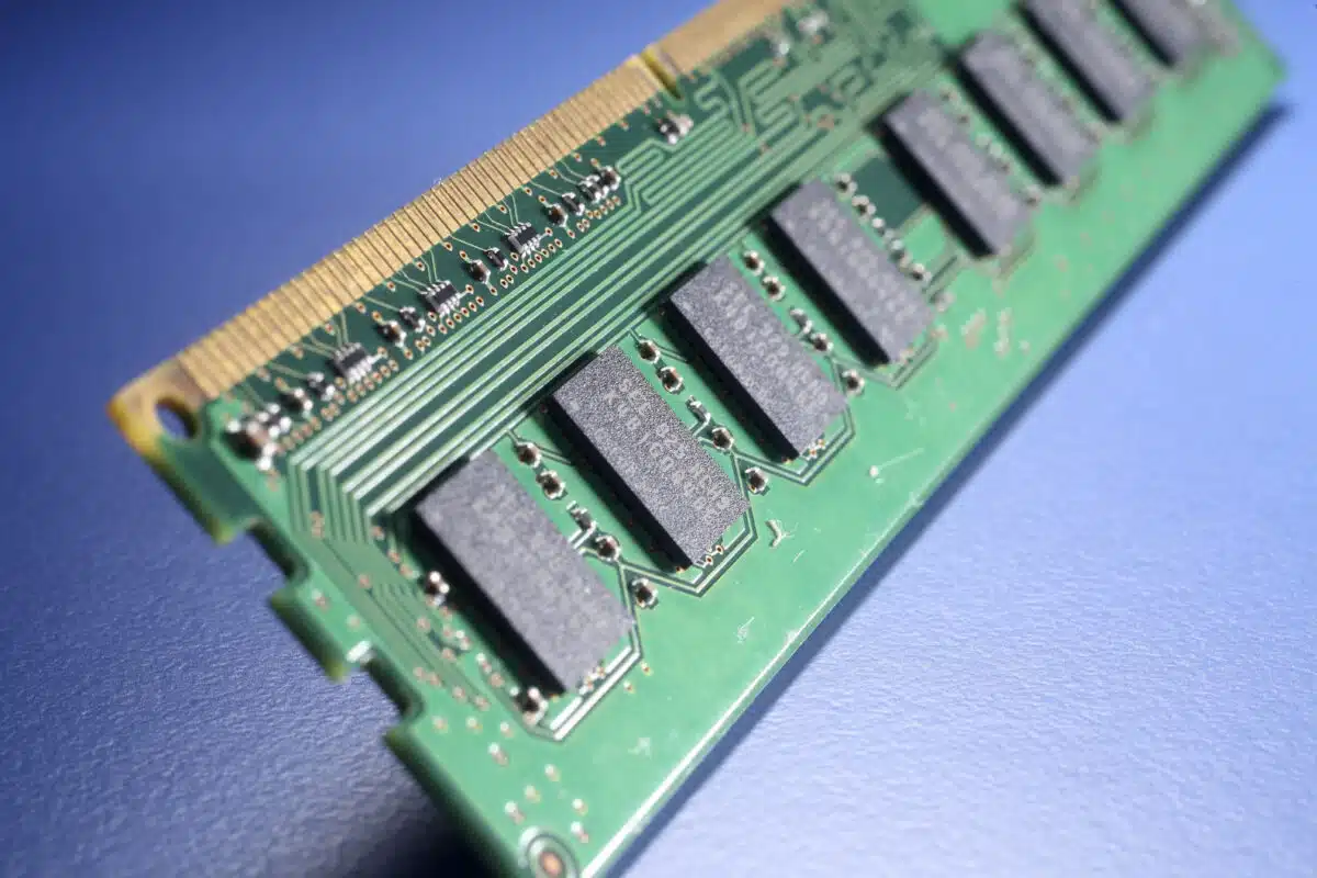
The SK Hynix 4Gb DDR3 series features an 8-bank internal design optimized for rapid, synchronized data transfers. Address and control signals are latched on the rising edge of CK, whereas data, data strobes, and write masks are sampled on both clock edges. It employs an 8n-bit prefetch with pipelined internal data paths to maintain high bus bandwidth[2][8].
Key Electrical and Operational Characteristics
- Density & Configurations: 4,294,967,296 bits organized as 512M words × 8 bits in a 78-ball FBGA[2]. The same die is also offered as 256M × 16 in a 96-ball FBGA (H5TQ4G63EFR).
- Speed Grades: Four marked grades are offered — -H9 (DDR3-1333 9-9-9), -PB (DDR3-1600 11-11-11), -RD (DDR3-1866 13-13-13) and -TE (DDR3-2133 14-14-14)[2]. Each grade also operates at the lower frequencies shown in its speed-bin table; note that SK Hynix verifies this lower-frequency operation by design and characterization rather than by production test[2], which is a point to capture in your component qualification plan. Optional downbinning to CL=7/9/11 requires tAA/tRCD/tRP of 13.125 ns and matching SPD programming. The November allocation is the -TE grade, the top bin in the family. Because any DDR3-2133 device also operates at the lower frequencies in its speed-bin table[2], a -TE part drops into sockets originally specified for -H9, -PB or -RD — which matters when the grade you designed around is the one that’s gone.
- Signal Integrity Features: Dynamic On-Die Termination, programmable driver strength via Extended Mode Registers, and ZQ calibration against an external 240 Ω reference. Typical initialization sets RON = RZQ/7 (34 Ω), RTT_Nom = RZQ/6 (40 Ω) and RTT_Wr = RZQ/2 (120 Ω)[2].
- Timing & Latency Controls: As the top -TE bin, the allocated parts support the full range: CAS Latency 5–11, 13 and 14; CAS Write Latency 5–10; and Additive Latency of 0, CL–1 or CL–2[2]. Lower speed grades support only a subset, so a -TE part will satisfy timing configurations that a -H9 or -PB part cannot.
- Temperature Grades: Commercial (-xxC, 0 °C to 95 °C), Industrial (-xxI, −40 °C to 95 °C) and Extended/Automotive (-xxK, −40 °C to 105 °C — labeled Automotive in the feature summary and Extended in the ordering table), specified as case temperature at the center/top of the package per JESD51-2[2]. Full specifications are guaranteed across these ranges, with the additional refresh conditions described below applying above 85 °C[2]. The allocated -TEI parts are the industrial grade, which is a superset of commercial — they drop into any socket a -xxC part was specified for.
- Low-Power Ordering Options: Beyond the standard -xxC / -xxI / -xxK grades, SK Hynix offers IDD6-screened low-power variants — -xxL (Commercial) and -xxJ (Industrial) — that cut self-refresh current from 13 mA to 10 mA at DDR3-1333 through DDR3-1600[2]. For battery-backed controllers, always-on gateways and any design where standby draw drives the power budget, these are worth quoting alongside the standard grades.
- Addressing & Page Size: Row addresses A0–A15, column addresses A0–A9, giving a 1 KB page size per bank[2]. Page size drives bank-interleaving strategy and your tFAW/tRRD budget — note the x16 variant’s 2 KB page carries different values, so timing figures ported from an x16 design won’t transfer directly.
For designs requiring high reliability operating above 85 °C, the refresh interval must shorten as case temperature rises. The standard average refresh interval (tREFI) is 7.8 µs from 0 °C to 85 °C, reduces to 3.9 µs from 85 °C to 95 °C, and further decreases to 1.95 µs from 95 °C to 105 °C[2]. This temperature-dependent scaling is managed by the memory controller — SK Hynix states that refresh commands should be doubled and then quadrupled in frequency, and self-refresh above 85 °C needs the Manual Self-Refresh mode with extended-range capabilities enabled via mode register MR2 (A6 = 0b, A7 = 1b)[2]. Designers targeting automotive applications should verify their controller’s refresh scheduling and MR2 settings early during system bring-up.
Accurate clock synchronization is essential when connecting these devices to system processors. To learn how timing jitter affects high-speed data buses, see our technical guide, “Clock Jitter Explained: Guide to System Timing Precision.”
Target Industries and Applications for 4Gb DDR3
The 4Gb (Gigabit) density point is considered the practical “sweet spot” for embedded platforms that need local memory for Linux kernels, graphical user interfaces, data packet buffering, and real-time processing.

Programmable Logic Controllers (PLCs), smart motor drives, and industrial touchscreen displays need dedicated memory to operate embedded real-time operating systems (RTOS). The industrial-grade SK Hynix 4Gb DDR3, specified for operation from −40 °C to 95 °C case temperature, offers the thermal margin and durability necessary for factory environments with wide temperature fluctuations.
Routers, edge switches, fiber optic line terminals, and M2M hubs depend heavily on 4Gb DDR3 Memory components for tasks like frame buffering, routing table lookups, and managing queues. The allocated -TE grade runs to DDR3-2133 with I/O capacitance of 1.4–2.1 pF, keeping loading predictable across wide, heavily-fanned data buses and supporting line-rate throughput in multi-port switches[2].
Medical devices, ranging from blood gas analyzers to multiparameter patient monitors, require a well-documented and traceable supply chain throughout their production, lasting beyond the lifespan of the silicon components. SK Hynix's monolithic DDR3 is known for its proven reliability. Obtaining a single controlled allocation via one channel means consistent date codes and lot traceability during manufacturing. This documentation meets audit requirements better than relying on a mix of open-market lots assembled under tight deadlines.
Supply Chain Strategy: Why Lock In November Allocations Today?
In 2026, legacy memory procurement requires proactive supply chain management. As consumer products rapidly adopt next-generation memory standards, established memory lines experience capacity displacement in wafer fabrication facilities worldwide. Relying on spot-market availability can cause delays, increased unit costs, or untracked stock exposure.
1. Hedging Against Rolling Component Constraints
Top-tier manufacturers tightly control DRAM wafer starts for mature technologies. Lead times vary from about 8 to 52 weeks, with allocated lines at the upper end of this range[13][14]. DDR3 faces constraints due to declining legacy manufacturing capacity, making long-term supply commitments harder to secure[14]. Suppliers increasingly refuse support for older nodes or only provide limited samples[15]. Securing volume allocations for November shipments now helps protect your production schedules from market disruptions. For more strategies on managing component pipelines, see our guide, Conquer the 52-Week Wait: Strategic Fixes for Long Lead Times, Shortages, and EOL Risk.
2. Ensuring Traceability and Eliminating Counterfeit Risk

3. Integrated Inventory Management
Suntsu integrates distribution with adaptable supply chain programs. Allocations secured now can be held, scheduled, and released based on custom production plans using our Vendor Managed Inventory and Inventory Management Solutions. This provides operations with complete visibility and inventory control, while safeguarding working capital.
Explore Sourcing and Engineering Services
As a hybrid distributor and manufacturer, Suntsu supports hardware projects across every tier of the product development lifecycle:
- Procurement and Sourcing Support:
- Coordinate end-of-life component buffers with our Obsolescence Management team.
- Resolve acute production line bottlenecks using our Shortage Mitigation workflows.
- Access comprehensive active and passive component lines through our trusted Global Sourcing network.
- Optimize overall product costs and identify alternate package pinouts using our BOM Analysis and Cost Reduction services.
- Component Engineering & Manufacturing:
- Ensure clock line stability by pairing your memory topologies with Suntsu Branded Products, including our specialized Frequency Control crystals and oscillators.
- Streamline hardware realization from bare board to finished product with our Full Box Build and turnkey assembly capabilities.
- Consult our technical archive, including our comprehensive Memory IC essentials: selecting the right components for your project, to simplify memory selection across every generation.
Secure Your SK Hynix 4Gb DDR3 Allocation
November allocation on the SK Hynix H5TQ4G83EFR-TEI is open for scheduling: 4 Gb (512M × 8), DDR3-2133, industrial temperature grade, in a 78-ball FBGA measuring 7.5 × 11.0 mm[2]. As the top speed bin, it also covers designs originally specified at DDR3-1866, 1600 or 1333. Reserve against your build schedule to lock in firm pricing and scheduled delivery.
Don’t let market shifts or rolling component constraints disrupt your production schedules. Contact the Suntsu team today to lock in your dedicated November allocation for SK Hynix H5TQ4G83EFR-TEI 4Gb DDR3 SDRAM.
FAQs
Because the H5TQ4G83EFR operates on a 1.5V SSTL_15 signal rail, maintaining clean eye diagrams requires strict impedance and length-matching control. Key layout rules include:
-
Trace Impedance: Route single-ended address/command lines at 50Ω and differential clock/d strobe pairs at 100Ω.
-
Length Matching: Match trace lengths within the data byte lane (DQ to DQS) to within ±5 mils to preserve timing margins.
-
Termination & ZQ Calibration: Utilize internal Dynamic On-Die Termination ODT and connect a precision 240Ω (±1%) resistor to the ZQ pin to automatically calibrate driver output impedance and termination values against temperature and voltage drift.
-
Reference Voltage (VREF): Maintain a quiet VREF supply rail (VDD/2) with dedicated decoupling capacitors isolated from high-current power traces.
The SK Hynix -TE speed grade operates natively at DDR3-2133 (14-14-14) but maintains full backward compatibility with lower speed bins, including DDR3-1866 (-RD), DDR3-1600 (-PB), and DDR3-1333 (-H9). The internal clock logic and mode registers (MR0) support programmable CAS Latencies (CL = 5 through 14). When dropping the -TE part into a legacy memory controller specified for a lower speed, the controller reads the internal Serial Presence Detect (SPD) table or programmatically configures the Mode Register Set (MRS) to match the target clock rate and timing parameters (tAA, tRCD, tRP). This enables immediate operation without requiring hardware layout modifications or substrate redesigns.
While modern consumer applications have migrated to DDR4 and DDR5, DDR3 and DDR3L maintain a massive footprint in embedded systems, industrial automation, medical equipment, and automotive electronics. These long-lifecycle applications rely on stable, validated architectures that do not require the higher bandwidth of newer standards. Furthermore, re-qualifications for newer memory architectures require substantial time and capital investment. Manufacturers continue to specify DDR3 because it offers a proven, cost-effective balance of performance, power consumption, and long-term ecosystem stability.
The primary difference lies in the operating voltage:
-
Standard DDR3: Operates strictly at 1.5V.
-
DDR3L (Low Voltage): Operates dual-voltage at 1.35V and 1.5V.
Because DDR3L is backward-compatible with 1.5V systems, it can run in a standard DDR3 socket. However, standard 1.5V DDR3 cannot operate in a system designed exclusively for 1.35V DDR3L without causing instability or system failure. Mixing both types on the same memory channel is generally not recommended, as the memory controller will typically default to 1.5V, eliminating the power-saving benefits of the DDR3L modules.
Major tier-one DRAM manufacturers have shifted significant wafer capacity away from legacy nodes (like DDR3) toward high-margin DDR5 and High Bandwidth Memory (HBM) for AI infrastructure. As a result, OEMs face sudden EOL notices, extended lead times, and allocation limits on legacy DDR3 parts. When a critical DDR3 IC reaches EOL unexpectedly, OEMs must either execute expensive redesigns or partner with hybrid distributors to secure long-term buffer stock, cross-referenced drop-in alternatives, or authorized legacy production lines.
Related Content
References
- Automotive Electronics Council. “AEC-Q100 Rev-G: Failure Mechanism Based Stress Test Qualification for Integrated Circuits” Available at: http://www.aecouncil.com/Documents/AEC_Q100_Rev_G_Base_Document.pdf
- SK Hynix. “4Gb DDR3 SDRAM — H5TQ4G83EFR / H5TQ4G63EFR” Available at: https://product.skhynix.com/download.do?attNo=1754&attTypeCd=TRT06
- JEDEC. “Addendum No. 1 to JESD79-3 – 1.35 V DDR3L-800, DDR3L-1066, DDR3L-1333, DDR3L-1600, and DDR3L-1866” Available at: https://www.jedec.org/standards-documents/docs/jesd79-3-1a01
- Micron Technology. “DDR3L SDRAM data sheet addendum (MT41K series)” Available at: https://mm.digikey.com/Volume0/opasdata/d220001/medias/docus/8923/557_MT41K256M16TW.pdf
- TrendForce. “Consumer DRAM Shortages Extend to DDR2 Products with Contract Prices Expected to Continue Rising in 3Q26” Available at: https://www.trendforce.com/presscenter/news/20260622-13112.html
- TrendForce. “Limited Capacity and Order Shifts Drive March Consumer DRAM Price Surge, Led by Sub-4Gb Products” Available at: https://www.trendforce.com/presscenter/news/20260407-13001.html
- SK Hynix. “4Gb DDR3L SDRAM — H5TC4G83CFR / H5TC4G63CFR” Available at: https://community.nxp.com/pwmxy87654/attachments/pwmxy87654/imx-processors/63257/1/Hynix_DDR3L_H5TC4G8(6)3CFR(Rev0.2).pdf
- JEDEC. “DDR3 SDRAM Standard (JESD79-3D)” Available at: https://www.jedec.org/standards-documents/docs/jesd-79-3d
- AMD (Xilinx). “Zynq-7000 SoC Overview (DS190)” Available at: https://www.digikey.com/htmldatasheets/production/1099073/0/0/1/zynq-7000-all-programmable-soc-overview.html
- Texas Instruments. “AM335x Sitara Processors datasheet” Available at: https://www.ti.com/lit/ds/symlink/am3358.pdf
- MD+DI. “Dealing with Electronic Component Obsolescence in Medical Devices” Available at: https://www.mddionline.com/components/dealing-with-electronic-component-obsolescence-in-medical-devices
- TrendForce. “Rapid Contract Price Surge Drives 1Q26 DRAM Industry Up 81% QoQ” Available at: https://www.trendforce.com/presscenter/news/20260601-13070.html
- Sourceability. “Q2 2026 Electronics Lead Times report” Available at: https://sourceability.com/post/q2-2026-lead-time-report-highlights
- VersaLogic. “Supply Chain Brief: Memory Market Conditions in 2026” Available at: https://www.versalogic.com/blog/supply-chain-brief-memory-market-conditions-in-2026/
- Avnet. “Riding the AI Supercycle: Navigating the 2026 Memory & Storage Market” Available at: https://www.avnet.com/integrated/resources/article/2026-memory-shortage-ai-supercycle/
- Astute Group. “Active Component Counterfeits Raise Sourcing Risks for OEMs” Available at: https://www.astutegroup.com/news/general/active-component-counterfeits-raise-sourcing-risks-for-oems/