
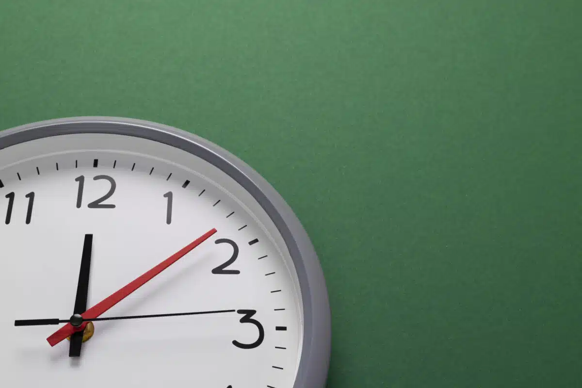
Clock Jitter vs. Phase Noise
A common source of confusion when choosing components is distinguishing between clock jitter and phase noise. In essence, they both measure the same phenomenon, but they do so using different mathematical perspectives.
- Clock Jitter (Time Domain): Jitter measures timing instability in the time domain with an oscilloscope. It quantifies how early or late a signal edge arrives.
- Phase Noise (Frequency Domain): Phase noise quantifies frequency instability with a spectrum analyzer. Rather than a sharp, narrow spike at the carrier frequency, it manifests as a “skirt” of unwanted frequencies extending from the carrier.
To determine the total RMS (Root Mean Square) phase jitter, engineers can mathematically integrate the phase noise over a specific frequency offset band, such as 12 kHz to 20 MHz. When evaluating components on our Frequency Control product pages, you will often see specifications for both, ensuring you have the data needed for your analysis.
Primary Causes of Clock Jitter
Jitter doesn’t occur randomly; instead, it results from physical and electrical environmental factors. The main causes can be grouped into two categories:
- Random Jitter (RJ)
Random jitter is inherently unpredictable and has no strict limit. It mainly originates from internal device physics, especially thermal noise. When electrons move through conductors or semiconductors, their thermal agitation causes small, random voltage fluctuations that directly lead to timing variations.
- Deterministic Jitter (DJ)
Deterministic jitter is bounded and predictable, usually stemming from external interference or specific system-level design flaws. Common culprits include:
- Crosstalk: Unwanted electromagnetic coupling between adjacent, parallel traces on the PCB.
- Power Supply Noise: Fluctuations, ripples, or “ground bounce” from poorly filtered power supplies.
- Electromagnetic Interference (EMI): External RF signals coupling into the clock routing.
How Jitter Negatively Impacts System Performance
Clock jitter effects go well beyond cluttered oscilloscope traces. When engineers complete a solid design, their main concern is uncovering a critical flaw that could hinder reliable manufacturing or operation.
Here is how clock jitter directly threatens your system:
Minimizing Clock Jitter in the PCB Design Phase
Reducing the need for board respins is a key performance metric for hardware engineers when bringing a design into production. To address jitter issues during layout, consider implementing these best practices:
- Isolate the Clock Domain: Keep clock traces as short as possible and route them far away from noisy, high-current switching signals.
- Optimize Power Integrity: Place low-ESR decoupling Capacitors as physically close to the oscillator’s power pins as possible to mitigate power supply noise.
- Impedance Matching: Ensure your clock traces are properly terminated to prevent signal reflections that distort the clock edge.
- Leverage Expert Analysis: If you are dealing with ultra-tight timing budgets, utilizing expert Board Characterization Services can help identify resonance and crosstalk issues before you ever manufacture a prototype.

Don’t let timing instability or component shortages jeopardize your next product launch. Request a quote today to secure high-performance, low-jitter oscillators and reliable sourcing solutions tailored to your project’s exact needs.
FAQs
Acceptable limits vary drastically depending on the protocol and the data rate. For instance, basic microcontrollers might tolerate several picoseconds of jitter, while a PCIe Gen 5 system strictly requires an RMS jitter of less than 0.15 ps (integrated from 12 kHz to 20 MHz). Using a component that exceeds these limits guarantees high bit error rates. If you are uncertain about protocol compliance, our Engineering Services team can help you select the exact Frequency Control products needed to meet your specific data rate requirements.
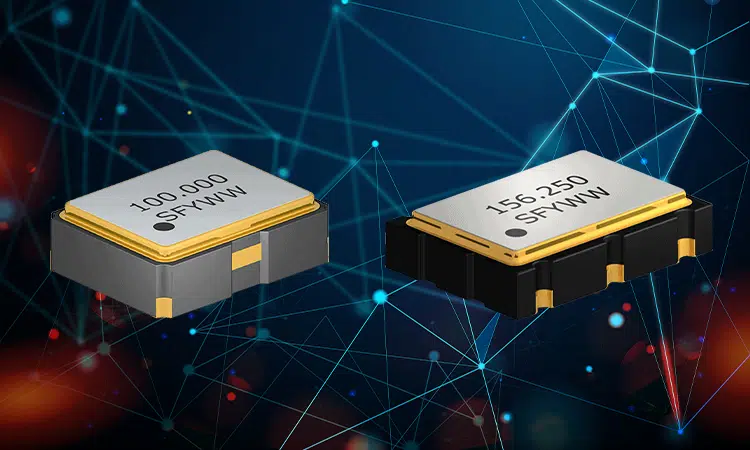
While MEMS (Micro-Electromechanical Systems) technology has made significant strides in recent years, traditional quartz crystal oscillators remain the gold standard for ultra-low phase noise and superior jitter performance in high-speed applications. Quartz possesses a naturally high Q-factor, making it highly stable. Suntsu specializes in manufacturing high-precision quartz Oscillators designed specifically to anchor demanding digital and RF systems.
Yes, every active component in your clock path introduces its own electrical noise, known as “additive jitter.” The total system jitter is not just the jitter of the source oscillator; it is calculated using the root-sum-square of the source jitter and the additive jitter of all buffers and Phase-Locked Loops (PLLs) in the chain.
Measuring femtosecond or sub-picosecond jitter is notoriously difficult because the intrinsic noise floor of a standard laboratory oscilloscope is often higher than the jitter of the oscillator itself. To get accurate readings, engineers must measure phase noise in the frequency domain using a dedicated Signal Source Analyzer (SSA) or Phase Noise Analyzer. If your team lacks this highly specialized equipment, Suntsu offers comprehensive Board Characterization Services to validate your timing architecture.
High-precision components require specialized manufacturing processes, rigorous testing, and specific raw materials. Because of this complexity, they are highly susceptible to global allocation and extended lead times. To combat this, Suntsu utilizes a hybrid business model. We manufacture our own robust line of timing components while leveraging our Independent Distribution network to provide rapid Shortage Mitigation, ensuring your production lines never go down.
Related Content