
Key Takeaways
- DRAM chips provide high-speed, volatile runtime execution memory for processors, but require continuous power and DRAM refresh cycles.
- Flash Memory provides non-volatile storage, divided into high-speed, byte-addressable NOR flash for code execution and high-density, block-addressable NAND flash for data storage.
- eMMC combines raw NAND flash with an integrated controller to handle wear leveling, bad block management, and host offloading over a standardized interface.
- MCP (Multi-Chip Package) vertically stacks DRAM and Flash into a single IC footprint, roughly halving the board area a discrete DRAM-plus-storage pair would occupy in space-constrained embedded systems.
What is a Memory IC?
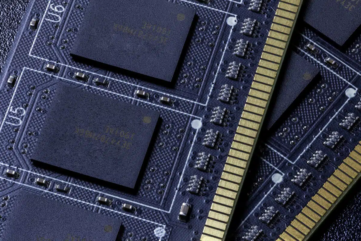
A memory integrated circuit (IC), often called a memory chip, is a specialized semiconductor device designed to store digital data via microscopic arrays of transistors, capacitors, or floating-gate structures. Memory ICs are essential, serving as the umbrella term for all solid-state silicon components that record, buffer, or retain binary instructions and system data within an electronic assembly.
Modern embedded architectures rely on different types of memory — split broadly into volatile and non-volatile memory — depending on whether data must persist when power is removed:
- Volatile Memory: Requires a continuous power supply to retain stored state. When power drops, the stored data is lost.
- Non-Volatile Memory: Retains data without power, preserving system firmware, application boot code, and user storage across power cycles.
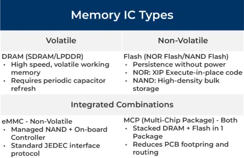
To build a reliable digital architecture, system designers combine different memory types into a functional memory hierarchy. The four primary families covered in this analysis are DRAM memory, raw Flash memory, eMMC modules, and MCP memory solutions.
DRAM — Fast, Volatile Working Memory
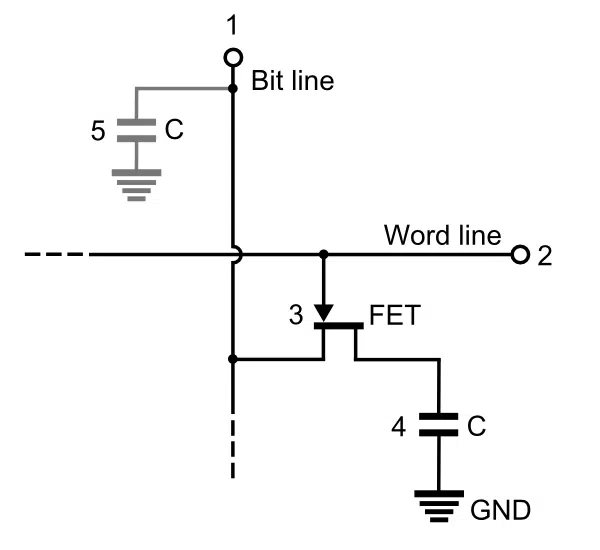
Dynamic Random-Access Memory (DRAM) serves as the primary system workspace, often called main memory, for host processors, system-on-chip (SoC) platforms, and microcontrollers. DRAM is a volatile memory technology engineered for ultra-fast, closely comparable read and write access times, enabling rapid execution of system instructions and high-bandwidth data buffering.
How DRAM Works and Why It Is Volatile
Typical Use as System Memory
System processors cannot read and write data directly to high-density non-volatile flash storage at the clock frequencies required for modern computational workloads. DRAM bridges this performance gap by acting as high-speed system RAM, commonly implemented as DDR memory. Common types include:
- DDR4 / DDR5 SDRAM: Used in high-performance compute, server memory, networking gear, and industrial automation gateways requiring high clock frequencies and high bandwidth.
- LPDDR (Low-Power DDR): Designed with lower operating voltages (such as LPDDR4x at 0.6V VDDQ[6][7]) and integrated power-saving sleep modes, making it ideal for mobile devices, IoT hardware, and compact battery-powered subassemblies.
- LPDDR5 / LPDDR5X / LPDDR6: The current low-power generations, driven by mobile and edge AI bandwidth demands. LPDDR5X drops I/O voltage further to 0.5 V[8], and JEDEC published the LPDDR6 standard (JESD209-6) in July 2025, moving to a dual sub-channel architecture with on-die ECC[9]. Specify these where sustained bandwidth, not just capacity, is the constraint — and confirm host SoC support early, since controller availability lags the standard.
Engineers specify DRAM as high-speed memory when a processor needs tens-of-nanoseconds access latency — DDR5-4800 delivers roughly 16 ns CAS latency and about 50 ns on a full random access[10]— together with effectively unlimited write endurance for temporary data processing.
Flash — Non-Volatile Storage (NAND vs. NOR at a Glance)
Flash memory is non-volatile semiconductor memory that traps electrical charge in the cell without requiring constant power. Retention is finite rather than permanent: JEDEC qualification (JESD47) targets roughly 10 years of data retention on a lightly-cycled device, falling toward 1 year once the part reaches its rated program/erase endurance[11][12][13]. Flash memory chips serve as the long-term memory of an embedded design, holding bootloader code, operating system images, configuration parameters, and user logs.
Flash architecture is divided into two main chip types: NOR Flash and NAND Flash.
Specification NOR Flash NAND Flash Primary Application Code Execution (Execute-In-Place) Mass Data Storage Memory Architecture Parallel cell wiring (byte access) Series cell wiring (Page/Block) Random Read Speed Very Fast Slow Write/Erase Speed Slow (~520ms per 128KB sector)[18] Fast (~3.5ms per 128KB block)[18] Storage Density Low to Medium (Mb to low Gb)[14][15] High to Ultra-High (Gb to Terabits)[16][17] Cost per Bit Higher Significantly Lower
NOR Flash Architecture
NOR flash connects individual memory cells in parallel between the bit line and ground. This configuration enables random, byte-level access, allowing host microcontrollers to fetch and execute instructions directly from the flash chip without loading the code into DRAM first. This capability is known as Execute-in-Place (XIP)[14].
NOR flash is optimized for lower densities where fast read speeds and instant-on execution are required, such as primary BIOS storage, automotive instrument clusters, and boot code memory.
NAND Flash Architecture
NAND flash memory connects memory cells in series, organizing data into structured pages (4 KB to 16 KB on current parts) and erase blocks that have grown sharply with 3D scaling — from a few hundred kilobytes on legacy SLC devices to 16–24 MB on modern 3D MLC and TLC[19][20][21]. Larger blocks are precisely why garbage collection and write amplification management have become non-trivial.
The erase asymmetry against NOR is dramatic in practice: a representative NAND device clears a 128 KB block in about 3.5 ms, while a comparable NOR device needs roughly 520 ms to erase a 128 KB sector[18] — close to a 150× difference. NOR’s erase penalty is why it is specified for code that is written once and read constantly, not for data that churns.
While NAND flash cannot perform byte-level Execute-in-Place operations, its tight cell layout yields much higher storage density and significantly lower cost per bit than NOR flash chips.
eMMC — Managed Flash With a Built-In Controller
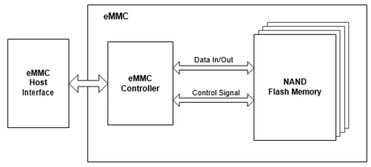
What eMMC Adds Over Raw NAND
The integrated controller acts as an abstraction layer between the host processor and the raw NAND flash arrays. It automatically handles background operations:
- Wear Leveling: Distributes write and erase cycles evenly across memory blocks to maximize package operational lifetime[24].
- Bad Block Management: Identifies corrupted factory blocks and re-maps defective flash areas transparently away from the host file system[24].
- Hardware ECC Engines: Detects and corrects bit flips on the fly during data read operations[24].
Simplifying Embedded Hardware Design
By standardizing on the parallel MMC interface bus — selectable at 1, 4, or 8 bits wide, with 8-bit the usual choice in embedded designs[24][25] — eMMC decouples the host processor from the internal evolution of NAND technology. If a memory vendor updates the underlying NAND flash architecture from 3D-TLC to a newer process node, the protocol command set stays constant and the package footprint is usually preserved. Re-qualification is still warranted, however: sustained throughput, endurance rating, and Ext_CSD behavior can all shift across a node transition, and eMMC is offered in more than one standard ball count[24][26].
This abstraction drastically simplifies board design, reduces software stack maintenance, and shortens development cycles for industrial control systems, automotive infotainment units, and smart edge devices.
A note on UFS:
eMMC is not the only managed-NAND option. JEDEC introduced Universal Flash Storage (UFS) as its intended successor, trading eMMC’s half-duplex parallel bus for a full-duplex serial interface with native command queuing[27]. UFS 4.1 was published in December 2024 and UFS 5.0 in February 2026[28][29], while eMMC has not gained a new performance tier since 5.1. eMMC remains the right choice for cost-sensitive, low-to-moderate bandwidth designs and for host SoCs without a UFS controller — but if your design is bandwidth-bound or expected to stay in production for a decade, UFS deserves evaluation. Our UFS vs. eMMC engineering guide compares the two in depth.
MCP — Combining Memory Types in One Package
What Is MCP Memory?
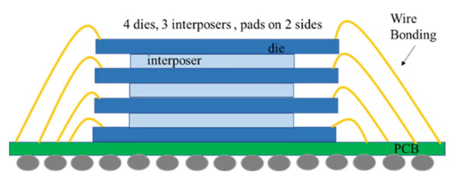
An MCP combines two or more heterogeneous memory devices—most commonly low-power volatile RAM (such as LPDDR4x or LPDDR5) paired with high-density non-volatile storage (such as SLC NAND or NOR)—into a unified component footprint[1]. Internal die interconnects are routed predominantly by ultra-fine wire bonding to a shared package substrate, with through-silicon vias (TSVs) appearing in higher-bandwidth and higher-density stacks[1][31].
Advantages of Stacking DRAM and Flash
Integrating different memory technologies like DRAM and Flash into an MCP provides key engineering benefits:
- PCB Area Savings: Stacking dies vertically roughly halves the board area consumed by the memory subsystem. A representative eMCP pairing 32 GB of eMMC with 16 Gb of LPDDR4 occupies a single 254-ball VFBGA at 11.5 × 13 mm — 149.5 mm²[32]. The discrete equivalents total 294.5 mm² before keepouts: a 153-ball e•MMC in an 11.5 × 13 mm outline (149.5 mm²)[26] plus a 200-ball LPDDR4 TFBGA at 10 × 14.5 mm (145 mm²)[7]. That is a saving of roughly 49%, and narrower-bus MCPs in smaller WFBGA outlines — Micron offers a 144-ball part at 8 × 9.5 mm — push the figure higher still[32].
- BOM and Sourcing Simplification: Hardware teams qualify and manage a single integrated memory part number instead of sourcing, tracking, and placing multiple distinct memory components.
- Signal Integrity and Trace Routing: Internal die-to-die interconnections shorten signal paths, reducing parasitic inductance, crosstalk, and high-frequency EMI noise[31].
- Lower Power Consumption: Reduced trace length translates to lower bus capacitance, helping extend operational runtimes in battery-powered edge hardware.
Which Memory Type Fits Your Design?
Selecting the right memory architecture requires analyzing key engineering trade-offs: data persistence, read/write latency, storage density, interface complexity, and total layout footprint.
Selection Factor DRAM Flash (NAND/NOR) eMMC UFS MCP Primary Role Execution/Working Code/Storage Managed Mass Storage High-bandwidth managed storage Combined RAM+Flash Volatility Volatile Non-Volatile Non-Volatile Non-Volatile Both (Combination) Access Speed Ultra-Fast Fast Read (NOR) Moderate to High Very High (serial, full duplex, command queueing) High Interface Type Parallel (DDR Bus) SPI/Parallel MMC Parallel Bus MIPI M-PHY Serial Independent LPDDR + NAND/eMMC interfaces on a shared ball map Board Space Medium Compact to Medium Compact BGA Compact BGA Ultra-Compact Design Complexity High (Trace Matching & Power Delivery Moderate Low (Controller Handles NAND) Moderate (high-speed serial routing; host controller required) Moderate (DDR routing rules still apply)
Engineering Decision Framework
Choosing the right memory for your application comes down to five decision points:
- When to Choose DRAM: Your system host processor requires fast, low-latency random access memory (RAM) to process real-time data buffers, run dynamic application logic, or render graphical UI displays.
- When to Choose Raw Flash: You need a cost-effective, non-volatile chip for direct code execution via NOR flash, or low-cost bulk data logging using raw SLC/MLC NAND flash where the host SoC already includes a dedicated hardware flash controller.
- When to Choose eMMC: Your design runs a complex operating system (such as Linux or Android) requiring gigabytes of reliable, high-density non-volatile storage without burdening the host processor with low-level NAND maintenance algorithms.
- When to Choose UFS: Your workload is storage-bandwidth-bound — edge AI inference, high-resolution imaging, automotive cockpit, or large OTA update payloads — and your host SoC provides a UFS controller. UFS also carries a longer forward roadmap than eMMC, which matters for products with extended production lifecycles.
- When to Choose MCP: Your system requires both high-speed runtime DRAM and non-volatile NAND/NOR flash, but strict enclosure dimensions limit available PCB surface area.
Optimize Your Memory Subsystem with Suntsu Engineering Support
Selecting the right memory IC requires balancing electrical specifications, bus speed, thermal thresholds, and long-term product lifecycle availability. Suntsu’s engineering team provides comprehensive component selection, technical cross-referencing, and global sourcing support to keep your production moving forward.
Search our component database using our Electronic Parts Search tool, or contact our application specialists directly to submit an RFQ and get a quote for your memory requirements.
FAQs
DRAM loses its contents the moment power is removed, so bootloader code, OS images, and configuration parameters have to live in non-volatile flash memory. Flash, in turn, can’t sustain the nanosecond-scale random access a processor needs at runtime — DDR5-4800 delivers roughly 16 ns CAS latency and about 50 ns on a full random access[10]. The two are complementary layers of the memory hierarchy, not substitutes.
Write amplification is the ratio of physical NAND writes to logical host writes, driven by the fact that flash erases in whole blocks but writes in pages. 3D scaling has pushed erase blocks from a few hundred kilobytes on legacy SLC parts to 16–24 MB on current MLC and TLC devices[19][20][21], so a small logical update can trigger a large read-modify-erase-write cycle. Higher amplification consumes endurance faster and makes garbage-collection behavior a real design variable — see our NAND flash overview for more.
Retention is finite and degrades with use. JESD47 targets roughly 10 years of retention on a lightly-cycled device, falling toward 1 year once the part reaches its rated program/erase endurance[11][12][13]. For long-dwell applications — archival loggers, spare units sitting on a shelf, products with extended field life — budget retention against expected P/E cycles rather than the headline 10-year figure.
No. Both are block-addressable and reached through a controller or command protocol, so there’s no byte-level XIP path. Designs that need instant-on execution typically pair a small NOR device for boot code with eMMC or NAND for bulk storage, or copy the image into DRAM at boot.
An MCP stacks heterogeneous dies in one BGA but exposes independent interfaces on a shared ball map — the LPDDR and NAND/eMMC buses are still routed and driven separately, so DDR trace-matching and power delivery rules continue to apply[1][31]. “eMCP” is the common industry term for the variant pairing managed eMMC with LPDDR, as opposed to raw NAND plus LPDDR[32]. No special combined host controller is required, only the controllers each interface already needs.
Related Content
References
- JEDEC. “MCP and Discrete e•MMC, e•2MMC, and UFS” Available at: https://www.jedec.org/standards-documents/docs/mcp-31201
- Zhang, X. et al. “Restore Truncation for Performance Improvement in Future DRAM Systems” Available at: https://people.cs.pitt.edu/~xianeizhang/doc/papers/restore_hpca16.pdf
- Bhati, I., Jacob, B. et al. “Enabling Scalable and Energy-Efficient DRAM Refresh” Available at: https://user.eng.umd.edu/~blj/papers/isca2015.pdf
- Cheng W-K, Shen P-Y, Li X-L. “Retention-Aware DRAM Auto-Refresh Scheme for Energy and Performance Efficiency” Available at: https://www.mdpi.com/2072-666X/10/9/590
- Nair, P. et al. “Refresh Pausing in DRAM Memory Systems” Available at: https://memlab.ece.gatech.edu/papers/TACO_2014_1.pdf
- JEDEC. “Low Power Memory: LPDDR” Available at: https://www.jedec.org/category/technology-focus-area/mobile-memory-lpddr-wide-io-memory-mcp
- Micron Technology. “Automotive LPDDR4/LPDDR4X SDRAM” Available at: https://mm.digikey.com/Volume0/opasdata/d220001/medias/docus/7180/MT53E1G32D2FW.pdf
- Takahashi, H. “LPDDR6” Available at: https://www.jedec.org/sites/default/files/JEDEC-PPT-16-9_LPDDR6_2025_hitakahashi.pdf
- JEDEC. “JEDEC Releases New LPDDR6 Standard to Enhance Mobile and AI Memory Performance” Available at: https://www.jedec.org/news/pressreleases/jedec%C2%AE-releases-new-lpddr6-standard-enhance-mobile-and-ai-memory-performance
- Vittal, S., Moinuddin, Q. “BARD: Reducing Write Latency of DDR5 Memory by Exploiting Bank-Parallelism” Available at: https://arxiv.org/pdf/2512.18300
- Liu, R.-S. et al. “Optimizing NAND Flash-Based SSDs via Retention Relaxation” Available at: https://www.usenix.org/system/files/conference/fast12/liu.pdf
- Macronix International. “AN0339: Program/Erase Cycling Endurance and Data Retention of NAND Flash Memories” Available at: https://www.macronix.com/Lists/ApplicationNote/Attachments/1920/AN0339V1-Endurance and Retention of NAND Flash.pdf
- Viking Technology. “AN0011: Flash Data Retention” Available at: https://www.vikingtechnology.com/wp-content/uploads/2021/03/AN0011_Flash-Data-Retention_RevB.pdf
- GigaDevice. “SPI NOR Flash — GD25 & GD55 series” Available at: https://www.gigadevice.com/product/flash/spi-nor-flash
- Macronix International. “Serial NOR Flash” Available at: https://www.macronix.com/en-us/products/NOR-Flash/Serial-NOR-Flash
- Blocks & Files. “Kioxia sampling highest capacity NAND chip at 2 terabits” Available at: https://blocksandfiles.com/2024/07/03/kioxia-2-terabit-nand/
- Kioxia Corporation / Sandisk. “New 3D Flash Memory Technology Achieves Industry’s Highest Bit Density for QLC NAND” Available at: https://www.kioxia.com/en-jp/about/news/2026/20260804-2.html
- Embedded.com. “Flash 101: NAND Flash vs NOR Flash” Available at: https://www.embedded.com/flash-101-nand-flash-vs-nor-flash/
- PC Perspective. “What Micron’s Upcoming 3D NAND Means for SSD Capacity, Performance, and Cost” Available at:
https://pcper.com/2016/02/what-microns-upcoming-3d-nand-means-for-ssd-capacity-performance-and-cost/ - flashdba. “Understanding Flash: Blocks, Pages and Program/Erases” Available at: https://flashdba.com/2014/06/20/understanding-flash-blocks-pages-and-program-erases/
- Cox, A. (Seagate; Chairman, JC-64.8). “JEDEC SSD Specifications Explained” Available at: https://www.jedec.org/sites/default/files/Alvin_Cox%20[Compatibility%20Mode]_0.pdf
- JEDEC. “e.MMC” Available at: https://www.jedec.org/standards-documents/technology-focus-areas/flash-memory-ssds-ufs-emmc/e-mmc
- JEDEC. “JESD84-B51: Embedded Multi-Media Card (e•MMC) Electrical Standard” Available at: https://www.jedec.org/standards-documents/docs/jesd84-b51
- Kingston Digital. “Embedded Multi-Media Card (e•MMC 5.1) EMMC16G-MW28-04B10 datasheet” Available at: https://mm.digikey.com/Volume0/opasdata/d220001/medias/docus/8856/EMMC16G-MW28-04B10.pdf
- BPM Microelectronics. “Mastering eMMC Device Programming” Available at: https://www.bpmmicro.com/mastering-emmc-device-programming/
- Alliance Memory. “ASFC4G31M-51BINTR” Available at: https://sg.rs-online.com/web/p/flash-memory/0425216
- Electronic Design / Kioxia America. “Explaining the Differences Between UFS and eMMC” Available at: https://www.electronicdesign.com/technologies/embedded/digital-ics/memory/article/55360218/kioxia-america-explaining-the-differences-between-ufs-and-emmc
- JEDEC. “Universal Flash Storage (UFS)” Available at: https://www.jedec.org/standards-documents/focus/flash/universal-flash-storage-ufs
- JEDEC. “JEDEC Announces Updates to Universal Flash Storage (UFS) and Memory Interface Standards” Available at: https://www.jedec.org/news/pressreleases/jedec%C2%AE-announces-updates-universal-flash-storage-ufs-and-memory-interface-0
- Arasan Chip Systems. “eMMC 5.1 Total Solution” Available at: https://www.arasan.com/wp-content/uploads/2016/05/eMMC-5-1-Total-Solution_Rev-1-3.pdf
- Intel Corporation. “Packaging Databook, Chapter 15: The Chip Scale Package (CSP)” Available at: https://www.intel.com/content/dam/www/public/us/en/documents/packaging-databooks/packaging-chapter-15-databook.pdf
- Micron Technology. “M2M MCP flyer” Available at: https://assets.micron.com/adobe/assets/urn:aaid:aem:02bdf02a-d165-4ef2-8747-2b150a545a84/renditions/original/as/flyer-m2m-mcp.pdf