
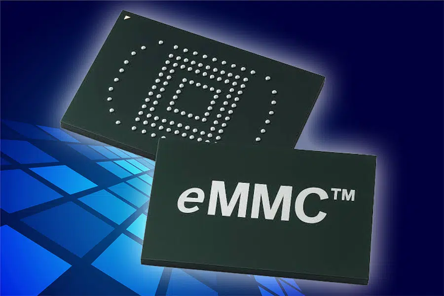

What is eMMC?
Embedded MultiMediaCard, or eMMC, is an advanced, highly integrated managed NAND memory solution designed specifically for embedded systems. Structurally, its architecture abstracts the inherent complexities of raw NAND flash management by bundling multiple components into a single, compact JEDEC-standard BGA package. This internal structural simplification provides several technical advantages over traditional discrete memory setups:
- NAND Flash Memory Cell Array: The main storage media can use Multi-Level Cell (MLC), Single-Level Cell (SLC), or Triple-Level Cell (TLC) configurations, optimized for specific performance requirements.
- Integrated Hardware Controller: An essential internal component that automatically manages fundamental flash tasks such as error correction code (ECC) generation, wear leveling (both dynamic and static), bad block handling, and garbage collection procedures.
- Standardized MMC Interface: A standard high-speed interface, usually conforming to eMMC 5.1 standards [1], communicates effortlessly with the host processor through an 8-bit parallel bus, simplifying the design process by abstracting complex raw flash timing details.
By offloading complex flash wear leveling and correction routines to the internal controller, eMMC offers a reliable, plug-and-play storage environment for boot and operation. This greatly reduces software driver complexity and speeds up time-to-market, unlike raw NAND components that need extensive software layers like Flash Translation Layers (FTL) running on the host processor.
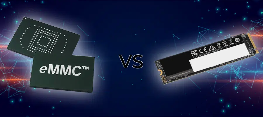
Key Factors When Choosing 4GB vs 8GB eMMC
Choosing between the eMMC 4GB and 8GB versions for a future deployment involves assessing various hardware and firmware metrics. Design teams need to go beyond initial code size and predict how the device will perform throughout its entire lifespan.

The main criterion for choosing storage is the size of the static code stack. A basic RTOS setup might need just a few megabytes, making a 4GB eMMC storage more than adequate. Conversely, newer embedded systems often use comprehensive Embedded Linux or Android Automotive distributions. These need significant storage space for root filesystems, dynamic libraries, containerized applications, and extra partitions for secure OTA firmware updates.
Flash memory cells wear out over time due to repeated program and erase cycles. Write endurance is usually measured in Terabytes Written (TBW). An 8GB eMMC contains twice the physical flash material as a 4GB module. With the same write workload, the eMMC 8GB device's internal controller has access to more blocks for wear leveling. As a result, upgrading to an 8GB part can effectively double the storage system's endurance headroom under the same write workload, since it doubles the available Terabytes Written (TBW) [3] - even if the software only uses a small part of the total capacity. (For applications needing even greater endurance, configuring the flash in pseudo-SLC mode is an alternative.)
Embedded sensors constantly record environmental data, network activity, or mechanical cycles, leading to frequent write operations. Since NAND flash requires large-block erasures before writing to individual pages, small, repeated writes cause high Write Amplification Factors (WAF). This results in the eMMC controller writing much more data to the physical cells than the host intended. Using a larger capacity eMMC reduces how often sectors are reused, which helps reduce cell degradation caused by high WAF.
4GB vs 8GB eMMC: Which Should You Choose?
To help cross-functional architecture and procurement teams compare these variables, the following structural comparison matrix highlights the main performance, lifecycle, and operational aspects of both capacities:
Technical Parameter 4GB eMMC Solution 8GB eMMC Solution Primary Target Application Lean RTOS, single-purpose microcontrollers, simple sensor nodes. Embedded Linux, complex Android modules, thick edge gateways. BOM Cost Efficiency Maximum upfront cost reduction for high-volume rollouts. Marginally higher unit cost but delivers better lifecycle ROI. OTA Update Compability Restricted; requires strict compression or single-partition switching. Excellent; supports robust A/B dual-partition rolling updates. Wear Leveling Pool Smaller; susceptible to faster degradation under heavy log cycles. Larger; spreads out write cycles to maximize overall MTBF. Data Logging Capacity Best for periodic, low-frequency status bursts. Suited for continuous high-rate telemetry and local databases.

eMMC Replacement Strategies for EOL Components
When broadline suppliers phase out high-volume legacy memory options, engineering teams need to implement precise, systematic replacement strategies to maintain ongoing production. This specialized cross-referencing process includes several crucial validation steps:
- Pin-to-Pin Compatibility Assessment: The replacement component should have the same ball grid array layout (like a standard 153-ball FBGA footprint) and exact package dimensions to ensure it can serve as a seamless drop-in replacement in existing PCB assemblies.
- Electrical Parameter Cross-Referencing: Engineers must carefully ensure that signaling voltages (Vcc and Vccq lines), clock frequencies, and bus speeds exactly match the timing requirements of the host application processor, without making any firmware changes.
- Firmware and Protocol Validation: Verifying that the eMMC specification version (such as v4.51, v5.0, or v5.1) fully supports backward compatibility with legacy operating system drivers [1].
- Custom Implementation Auditing: Reviewing the peripheral subsystems of the hardware schematic involves validating timing margins using low-noise Crystals and specialized high-frequency Oscillators that ensure stable system reference clocks.
Suntsu Electronics answers this industrial pain point directly. By operating under a unique hybrid model combining intensive global procurement agility with comprehensive in-house Engineering Services, Suntsu designs, cross-references, and manufactures high-reliability memory components. When a standard broadline part becomes unavailable, Suntsu’s team can provide highly reliable Custom Components engineered to serve as drop-in legacy alternatives, eliminating the need for expensive board redesigns and minimizing structural qualification disruptions.
Strategic Sampling and Replacement Options
When transitioning away from EOL or high-lead-time eMMC components, securing engineering samples early is critical to maintaining design schedules.
- Immediate & Near-Term Availability: JSC 4GB eMMC samples are available immediately to accelerate prototype testing, with 8GB eMMC samples becoming available by the end of this month (August 2026).
- Standardized Footprint: Available in standard 153 FBGA packaging, these drop-in replacements minimize hardware redesigns while adhering strictly to the eMMC 5.1 standard.
- Performance & Durability: Supporting high-speed HS400 modes, these solutions offer reliable performance for demanding applications and come in both commercial and industrial temperature grades (-40°C to +85°C).
For full electrical specs, timing diagrams, and pinouts, download the official 4GB JSC eMMC datasheet linked below, or contact us for more information about 8GB eMMC.


Ready to secure a reliable, long-term 4GB or 8GB eMMC supply for your embedded design? Contact our engineers today to review your Bill of Materials, cross-reference EOL parts, or request engineering samples.
FAQs
No. eMMC and UFS are pin-incompatible and electrically distinct. eMMC uses a half-duplex parallel interface (typically 8 data lines + clock/command), whereas UFS relies on high-speed serial differential TX/RX lanes running over MIPI M-PHY and UniPro protocols. Migration requires a hardware redesign and host processor support.
Yes. UFS requires a dedicated UFS host controller and MIPI M-PHY physical layer IP on the SoC. If your application processor or MCU only integrates an SD/eMMC host controller, it cannot interface directly with UFS without an external bridge or protocol conversion chip.
eMMC generally consumes less idle power and active power at lower clock rates, making it highly efficient for intermittent, low-duty-cycle logging. However, UFS is significantly more energy-efficient per gigabyte transferred (mJ/GB) due to its higher bandwidth. Under sustained heavy I/O, UFS generates more heat and requires careful thermal design and PMIC rail considerations.
UFS relies on the SCSI architecture with Tagged Command Queuing (and Multi-Circular Queues in UFSHCI 4.0+). This allows the controller to accept, buffer, and reorder out-of-order execution tasks optimized for internal NAND pages. eMMC 5.1 Command Queuing is constrained by a half-duplex shared data bus, creating turnaround overhead during mixed operations.
Both storage types are commonly integrated into surface-mount Ball Grid Array (BGA) packages. However, their BGA ballout grids (e.g., 153-ball eMMC vs. 153-ball or 176-ball UFS) differ in signal assignations and differential routing requirements.
Related Content
References
[1] JEDEC. “Embedded Multi-Media Card (eMMC) Electrical Standard, JESD84-B51B” Available at: https://www.jedec.org/standards-documents/docs/jesd84-b51
[2] ATP. “What is eMMC / SSD? The difference between managed and raw NAND” Available at: https://www.atpinc.com/blog/what-is-emmc-ssd-difference-between-managed-raw-nand
[3] Kingston. “eMMC Life-Cycle: Estimating, Validating & Monitoring” Available at: https://www.kingston.com/en/blog/embedded-and-industrial/emmc-lifecycle
[4] KIOXIA. “Analyzing Managed Flash Device Lifetime Reliability: TBW, WAF and NAND Flash Endurance” Available at: https://americas.kioxia.com/content/dam/kioxia/en-us/business/memory/mlc-nand/asset/KIOXIA_TBW_WAF_NAND_Endurance_Technical_Brief.pdf
[5] Suntsu Electronics. “Electronic Component Shortage Mitigation” Available at: https://suntsu.com/independent-distribution/shortage-mitigation/