
R7S721034VCBG#AC0
| Part Description |
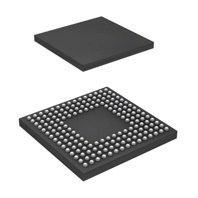
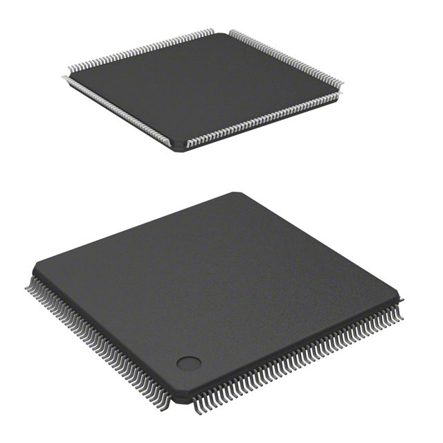
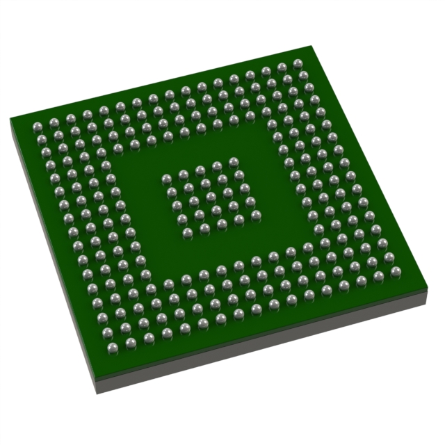
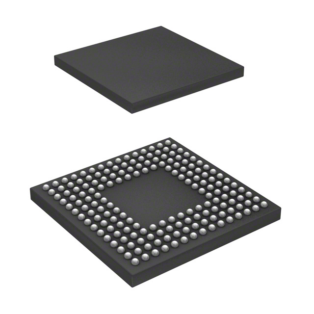
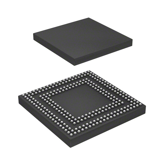
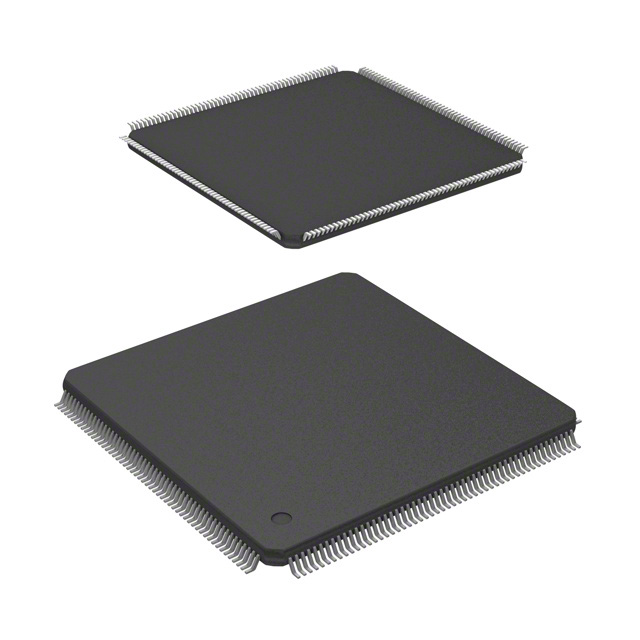
ARM® Cortex®-A9 Microprocessor IC RZ/A1LC 1 Core, 32-Bit 400MHz 176-LFBGA (8x8) |
|---|---|
| Quantity | 730 Available (as of October 8, 2026) |
| Product Category | Microprocessors |
|---|---|
| Part Series | R7S721034 |
| Manufacturer | Renesas Electronics Corporation |
| Manufacturing Status | Active |
| Manufacturer Standard Lead Time | 18 Weeks |
| Datasheet |
Specifications & Environmental
| Co-Processors/DSP | Multimedia; NEON™ MPE | Core Processor | ARM® Cortex®-A9 | Device Package | 176-LFBGA (8x8) | ||
|---|---|---|---|---|---|---|---|
| Display & Interface Controllers | VDC | ECCN | 3A991A2 | Ethernet | 10/100Mbps | ||
| Graphics Acceleration | Yes | HTS Code | 8542.31.0001 | Moisture Sensitivity Level | 3 (168 Hours) | ||
| Mounting Method | Surface Mount | Mounting Type | Surface Mount | Number of Cores/Bus Width | 1 Core, 32-Bit | ||
| Operating Temperature | -40°C ~ 85°C (TA) | Package / Case | 176-LFBGA | RAM Controllers | SDRAM, SRAM | ||
| REACH Compliance | REACH Unaffected | RoHS Compliance | ROHS3 Compliant | Speed | 400MHz | ||
| Supplier Device Package | 176-LFBGA (8×8) | USB | USB 2.0 (2) | Voltage – I/O | 1.2V, 3.3V |
Overview of R7S721034VCBG#AC0 – IC MPU RZ/A1LC 400MHZ 176LFBGA
The R7S721034VCBG#AC0 is an ARM® Cortex®-A9 microprocessor IC featuring a single 32-bit core running at up to 400 MHz in a 176‑LFBGA (8×8 mm) package. It targets industrial and general-purpose embedded applications that require a balanced combination of compute, display and connectivity functions.
Designed with integrated peripherals and on‑chip memory controllers, this device delivers system-level integration for LCD control, multimedia processing and networked embedded systems while supporting extended operating temperatures from -40 °C to 85 °C.
Key Features
- CPU ARM® Cortex®-A9 single core, 32‑bit, up to 400 MHz for general-purpose embedded processing.
- Memory and Cache 2 MB on-chip RAM; primary cache (64 KB: 32 KB instruction / 32 KB data), TLB 128 entries, and 128 KB secondary L2 cache (CoreLink™ L2C-310).
- Peripherals and DMA DMAC with 16 channels and an external address/data bus for flexible data movement and system interfacing.
- Display High-resolution display controller VDC5 supporting XGA (1024 × 768) for LCD control and graphical interfaces.
- Analog On-chip 12‑bit ADC with 8 channels for sensor and analog input acquisition.
- Connectivity Integrated Ethernet 10/100 Mbps, 2 × USB 2.0 (host and peripheral, high-speed support), 2 × CAN, plus multi-channel serial interfaces (12 CSI, 5 UART, 3 SPI, 4 I2C).
- Timers and I/O Multiple timers including five 16‑bit timers, two 32‑bit timers, one watchdog, up to 100 I/O ports and 109 external interrupt pins for real-time control.
- Power and Supply Operating supply rails documented across VCC, PVCC, PLLVCC and other domain voltages; primary operating voltage range noted as 3.0 to 3.6 V.
- Package and Thermal 176‑terminal LFBGA, 8 × 8 mm footprint, 0.5 mm pitch, max mounting height 1.4 mm; industrial operating temperature −40 °C to 85 °C.
- Environmental RoHS compliant.
Typical Applications
- Industrial Control Real-time control and monitoring systems where industrial temperature range and integrated communications are required.
- LCD and HMI Systems Display controller and graphics acceleration support XGA panels and graphical user interfaces for equipment control panels.
- Connectivity Gateways Ethernet, USB and CAN interfaces enable networked embedded devices and protocol bridging in connected applications.
- Multimedia and Sensor Processing NEON™ multimedia processing engine and ADC channels support audio/video preprocessing and multi-channel sensor acquisition.
Unique Advantages
- Integrated compute and graphics: Combines an ARM® Cortex®-A9 core with display controller and graphics acceleration to simplify HMI and multimedia designs.
- Comprehensive I/O set: Rich peripheral mix (Ethernet, USB, CAN, CSI, UART, SPI, I2C) reduces external components and BOM for connectivity-focused systems.
- Memory hierarchy for performance: On-chip RAM plus multi-level cache (64 KB primary, 128 KB L2) and TLB support reduce external memory dependency and improve deterministic performance.
- Industrial ready: Specified operating temperature range of −40 °C to 85 °C and industrial qualification make it suitable for harsh environments.
- Small-footprint package: 176‑LFBGA 8×8 mm package enables compact board designs while providing a high pin count for system integration.
- Standards-compliant supply options: Documented supply domains and voltages support disciplined power sequencing and multi-voltage system design.
Why Choose R7S721034VCBG#AC0?
The R7S721034VCBG#AC0 positions itself as an integrated MCU-class MPU for embedded systems that require balanced processing, graphics and connectivity in a compact industrial-grade package. Its ARM® Cortex®-A9 core, layered cache architecture and on-chip peripherals simplify system architecture and reduce external component count.
This device is well suited for designers building industrial control units, HMI panels, connectivity gateways and multimedia-enabled embedded products who need a reliable, RoHS‑compliant microprocessor with broad peripheral integration and a documented operating temperature range.
Request a quote or submit an inquiry to receive pricing, availability and technical support information for R7S721034VCBG#AC0.





















Date Founded: 2002
Headquarters: Koto City, Tokyo, Japan
Employees: 21,000+
Revenue: $10 Billion
Certifications and Memberships: ISO9001:2015, IATF16949:2016


