
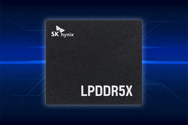
Key Takeaways
- High Data Throughput: Up to 8533 Mbps per pin in Bank Group (BG) mode with a 4:1 WCK:CK ratio, for about 68.3 GB/s peak across four x16 channels[1].
- Extended Temperature Range: Rated for -40°C to +105°C operating case temperature (Q-grade), matching the JEDEC Automotive Grade 2 range. Sister parts cover -40°C to +95°C (V-grade) and -40°C to +125°C (P-grade)[1].
- Flexible Voltage Rails: VDD1 = 1.8V, VDD2H = 1.05V, VDD2L = 0.9V, and VDDQ = 0.5V. VDDQ drops to 0.3V when I/O voltage scaling (DVFSQ) is enabled for lower-speed operation[1].
- Compact FBGA Footprint: 441-ball, 14mm × 14mm, 0.65mm-pitch FBGA with a 1.1mm maximum height, lead- and halogen-free[1].
- Targeted Applications: Automotive cockpit and ADAS platforms, edge AI and robotics, industrial automation, and rugged portable systems.

What Does the “LPDDR5X” Specification Mean for High-Performance Hardware?

What Are the Key Technical Specifications of the H58G66BK8QX105N?
The SK hynix H58G66BK8QX105N is an 8GB (64Gb) device organized as four independent x16 channels (A–D). Each channel is served by one 16Gb x16 die with a single chip select (4CH 1CS)[1].
Parameter Specification Details Manufacturer SK hynix Part Number H58G66BK8QX105N (datasheet base P/N H58G66BK8QX105; Q = -40°C to +105°C)[1] Density 64Gb / 8GB (four x16 channels; four 16Gb dies)[1] Maximum Speed 8533 Mbps per pin (LPDDR5X-8533); ~68.3 GB/s peak[1] Operating Voltages VDD1 = 1.8V, VDD2H = 1.05V, VDD2L = 0.9V, VDDQ = 0.5V (0.3V with DVFSQ)[1] Operating Temperature -40°C to +105°C (case)[1] Package / Ball Count 441-ball FBGA, 14.00 × 14.00mm, 0.65mm pitch, 1.1mm max height, lead- and halogen-free[1] Supported Bank Modes BG mode (4 bank groups × 4 banks) above 3200 Mbps; 16B mode (16 banks) at ≤3200 Mbps[1] Burst Length 16 and 32[1]
The device runs from multiple power rails to balance performance against standby current. It uses a differential command/address clock (CK_t/CK_c) and differential data clocks (WCK_t/WCK_c). In 4:1 mode the command clock runs at a quarter of the data clock rate, for example 1066 MHz for an 8533 Mbps device, which keeps timing tight at full speed[1].
For complete supply chain support, review our authorized line card and explore Suntsu’s global sourcing capabilities for active and legacy memory chips.
What Applications and Processor Platforms Are Best Suited for This LPDDR5X Part?
The Q-grade’s -40°C to +105°C rating matches the JEDEC Automotive Grade 2 temperature range[1], making the part suitable for demanding operational environments. SK hynix has also earned ISO 26262 ASIL-D functional-safety certification for its latest automotive LPDDR5X[6]; confirm part-level safety and AEC-Q100 documentation for this specific device with SK hynix before relying on either in a safety case. Typical applications include:

Automotive Cockpit & ADAS
Advanced infotainment units, digital clusters, and sensor-fusion systems requiring extended thermal performance. NVIDIA’s DRIVE AGX Thor, for example, moved to LPDDR5X and delivers 273 GB/s of memory bandwidth, up from 205 GB/s with LPDDR5 on the previous-generation Orin[7].

Edge AI & Machine Learning Accelerators
High bandwidth allows local AI inference engines to process image streams and sensor inputs rapidly without memory bottlenecks. NVIDIA’s Jetson Thor robotics modules, for instance, use a 256-bit LPDDR5X interface delivering 273 GB/s[8].

Rugged Portable & Handheld Computing
One 14mm × 14mm package carries a full 64-bit LPDDR5X interface, cutting component count on space-constrained boards used in field instruments, rugged tablets, and portable test equipment.

Industrial Automation & Robotics
Rugged industrial controllers requiring reliable low-power SDRAM operating across wider thermal ranges. Choose the V-, Q-, or P-grade variant to match the enclosure’s worst-case case temperature[1].
Whatever the platform, the processor’s memory controller must support LPDDR5X in a x64, four-channel configuration, and the part should appear on the SoC vendor’s memory qualification list before design-in.
When sourcing SK hynix memory or planning new designs, OEMs often face lead-time variations and market allocations. Suntsu offers proactive excess inventory solutions and second sourcing solutions to keep production lines running smoothly.
How Does LPDDR5X Compare to Standard LPDDR5 or DDR5 Memory?
Selecting the proper memory technology depends on system priorities regarding speed, power consumption, and physical footprint.
| Feature / Specification | LPDDR5X | LPDDR5 | DDR5 |
|---|---|---|---|
| Primary Target Application | Smartphones, automotive ADAS/infotainment, edge AI, AR/VR[2] | Mobile, automotive, low-power embedded[9] | Servers, desktops, laptops, workstations[11] |
| Max Data Rate (Per Pin) | 8533 Mbps (JESD209-5B); up to 10,600 Mbps in current products[2][4][5] | 6400 Mbps[2][9] | 4800 Mbps at launch; JEDEC timings to 8800 Mbps[10][11] |
| Supply Voltages | VDDQ 0.5V (0.3V with DVFSQ); VDD2H 1.05V; VDD2L 0.9V; VDD1 1.8V[1] | Same rail structure; VDDQ 0.5V nominal (0.3V at low speed)[1] | VDD/VDDQ 1.1V; VPP 1.8V[11] |
| Channel Architecture | x16 channel per die (x8 byte mode optional)[3] | x16 channel per die (x8 byte mode optional)[3] | Two independent 32-bit subchannels per DIMM (40-bit with ECC)[11] |
| Power Management | DVFSC, DVFSQ, Enhanced DVFSC, deep sleep[1] | DVFSC, DVFSQ, deep sleep[1] | On-module PMIC[11] |
| Signal Integrity | TX/RX equalization; programmable ODT[1][2] | Programmable ODT[1] | Decision feedback equalization (DFE)[11] |
| Reliability Features | Link ECC (required device support); Adaptive Refresh Management[1][2] | Link ECC[1] | On-die ECC; same-bank refresh; Per-Row Activation Counting[10][11] |
| Form Factor | Soldered-down BGA or PoP; CAMM2 (LPCAMM2) modules[12] | Soldered-down BGA or PoP; CAMM2 (LPCAMM2) modules[12] | DIMM, SODIMM, CUDIMM, CAMM2, or memory-down[11] |
- LPDDR5X vs. LPDDR5: LPDDR5 tops out at 6400 Mbps, while LPDDR5X extends to 8533 Mbps[2]. JEDEC simplified the LPDDR5X bank architecture by dropping 8-bank (8B) mode, keeping BG mode for rates above 3200 Mbps and 16B mode for 3200 Mbps and below[1][2]. SK hynix notes this device can still run 8B mode at 6400 Mbps and below[1].
- LPDDR5X vs. Standard DDR5: DDR5 runs at 1.1V VDD/VDDQ and is usually deployed on modules with an on-board PMIC[11]. LPDDR5X I/O runs at 0.5V (0.3V with DVFSQ)[1] and sits close to the processor on short point-to-point routes, which helps it reach high data rates at lower I/O power. The trade-off is flexibility: soldered LPDDR5X can’t be upgraded in the field, while socketed DDR5 makes it easier to add capacity.
If your current design relies on legacy memory types or faces component obsolescence, read our guide on strategies for mitigating electronics components obsolescence or review our analysis on semiconductor fab capacity trends.
Strategic Implementation of LPDDR5X Memory
The SK hynix H58G66BK8QX105N brings LPDDR5X’s 8533 Mbps data rate and roughly 68 GB/s of peak bandwidth to designs that must operate from -40°C to +105°C, making it a strong fit for automotive, edge AI, and industrial platforms[1]. Adopting it is a platform decision, not a drop-in swap: the processor’s memory controller and PHY must support LPDDR5X, and the board needs matching layout and power rails. Confirming the part on your SoC vendor’s memory qualification list and choosing the right temperature grade (V, Q, or P) early in the design cycle prevents costly surprises later[1]. Pairing those decisions with a dependable supply chain partner helps teams secure the LPDDR5X performance they need without putting production schedules at risk.
Need the H58G66BK8QX105N or other SK hynix memory for your next build? Request a quote, and Suntsu will help you secure LPDDR5X supply from prototype through full production.
FAQs
Link ECC is an error-correction feature that protects data as it travels between the processor and the memory. All LPDDR5X devices must support Link ECC, but the processor’s memory controller has to enable it. The H58G66BK8QX105N also supports write data masking and DC-balancing Data Bus Inversion (DBIdc) through its DMI pin. DBIdc reduces I/O switching activity, which helps with power and signal integrity. Together, these features improve data reliability at the high speeds LPDDR5X runs at.
The H58G66BK8QX105N uses four supply rails: VDD1 at 1.8V, VDD2H at 1.05V, VDD2L at 0.9V, and VDDQ at 0.5V. VDDQ drops to 0.3V when I/O voltage scaling (DVFSQ) is enabled for lower-speed operation. The multi-rail design lets the device balance peak performance against standby current. Board designers need to plan power delivery for each rail, including the ability to switch VDDQ levels if the system will use DVFSQ.
LPDDR5X uses two separate differential clocks: a command/address clock (CK_t/CK_c) and a data clock (WCK_t/WCK_c). The WCK:CK ratio describes how fast the data clock runs relative to the command clock. In 4:1 mode, the command clock runs at a quarter of the data clock rate. For an 8533 Mbps device, that puts the command clock at about 1066 MHz. Keeping the command clock slower while the data clock runs at full speed helps keep timing tight and manageable at the device’s maximum data rate.
DVFSC (dynamic voltage and frequency scaling for the core) and DVFSQ (the same for I/O) let the device run at lower voltages when the system doesn’t need full bandwidth, cutting power consumption. The trade-off is speed. DVFSC caps operation at 1600 Mbps, and DVFSQ is specified for operation up to 3200 Mbps, with VDDQ dropping from 0.5V to 0.3V. The device also supports Enhanced DVFSC. These modes are useful for battery-powered or thermally constrained systems that spend much of their time at low workloads.
The device supports Bank Group (BG) mode, organized as four bank groups of four banks each, for data rates above 3200 Mbps. At 3200 Mbps and below, it can run in 16-bank (16B) mode. JEDEC simplified the LPDDR5X bank architecture by dropping the 8-bank (8B) mode used in LPDDR5, but SK hynix notes this device can still run in 8B mode at 6400 Mbps and below. The device supports burst lengths of 16 and 32.
Related Content
References
- SK hynix. “H58G66BK8V(Q&P)X105 8GB LPDDR5x 441ball FBGA Specification” Available on request
- JEDEC. “JEDEC Publishes New and Updated Standards for Low Power Memory Devices Used in 5G and AI Applications” Available at: https://www.jedec.org/news/pressreleases/jedec-publishes-new-and-updated-standards-low-power-memory-devices-used-5g-and-ai
- JEDEC. “JESD209-5C: Low Power Double Data Rate (LPDDR) 5/5X” Available at: https://www.jedec.org/standards-documents/results/jesd209-5
- B. Murdock. “LPDDR6 A Deep Dive Into the JEDEC Press Release” Available at: https://www.jedec.org/sites/default/files/Brett Murdock_FINAL_Mobile_2024.pdf
- Qualcomm. “Snapdragon 8 Elite Gen 5 Product Brief” Available at: https://www.qualcomm.com/content/dam/qcomm-martech/dm-assets/documents/Snapdragon-8-Elite-Gen-5-product-brief.pdf
- SK hynix. “SK hynix LPDDR5X Achieves ASIL-D, the Highest Automotive Memory Functional Safety Rating” Available at: https://news.skhynix.com/en/sk-hynix-lpddr5x-earns-top-automotive-memory-safety-rating/
- Nvidia. “Accelerate Autonomous Vehicle Development with the NVIDIA DRIVE AGX Thor Developer Kit” Available at: https://www.edge-ai-vision.com/2025/09/accelerate-autonomous-vehicle-development-with-the-nvidia-drive-agx-thor-developer-kit/
- Nvidia. “NVIDIA Jetson Thor” Available at: https://www.nvidia.com/en-us/autonomous-machines/embedded-systems/jetson-thor/
- JEDEC. “JEDEC Updates Standard for Low Power Memory Devices: LPDDR5” Available at: https://www.jedec.org/news/pressreleases/jedec-updates-standard-low-power-memory-devices-lpddr5
- JEDEC. “EDEC Updates JESD79-5C DDR5 SDRAM Standard: Elevating Performance and Security for Next-Gen Technologies” Available at: https://www.jedec.org/news/pressreleases/jedec-updates-jesd79-5c-ddr5-sdram-standard-elevating-performance-and-security
- Kingston Technology. “DDR5 Memory Standard: An Introduction to the Next Generation of DRAM Module Technology” Available at: https://www.kingston.com/en/blog/pc-performance/ddr5-overview
- JEDEC. “JESD318-F0-RCE: LPDDR5/5X Compression Attached Memory Module (CAMM2) Raw Card E Annex” Available at: https://www.jedec.org/standards-documents/results/4_01_02_11