
T4241NSN7TTB
| Part Description |
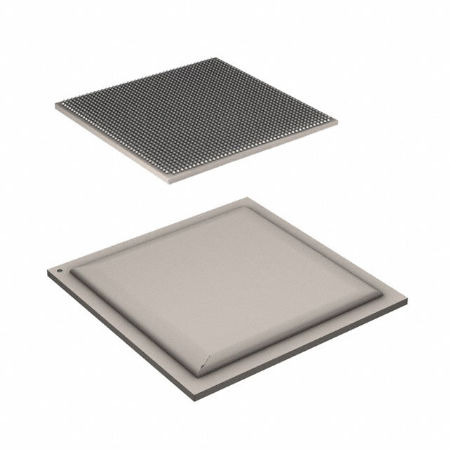
PowerPC e6500 Microprocessor IC QorIQ T4 24 Core, 64-Bit 1.8GHz 1932-FCPBGA (45x45) |
|---|---|
| Quantity | 257 Available (as of October 8, 2026) |

| Product Category | Microprocessors |
|---|---|
| Part Series | T4241 |
| Manufacturer | NXP USA Inc. |
| Manufacturing Status | Active |
| Manufacturer Standard Lead Time | 18 Weeks |
| Datasheet |
Specifications & Environmental
| Core Processor | PowerPC e6500 | Device Package | 1932-FCPBGA (45x45) | ECCN | 5A002A1 | ||
|---|---|---|---|---|---|---|---|
| Ethernet | 1Gbps (13), 10Gbps (2) | Graphics Acceleration | No | HTS Code | 8542.31.0001 | ||
| Moisture Sensitivity Level | 3 (168 Hours) | Mounting Method | Surface Mount | Mounting Type | Surface Mount | ||
| Number of Cores/Bus Width | 24 Core, 64-Bit | Operating Temperature | 0°C ~ 105°C (TA) | Package / Case | 1932-BBGA, FCBGA | ||
| RAM Controllers | DDR3, DDR3L | REACH Compliance | REACH Unaffected | RoHS Compliance | ROHS3 Compliant | ||
| SATA | SATA 3Gbps (2) | Security Features | Boot Security, Cryptography, Secure Fusebox, Secure Debug, Tamper Detection, Volatile key Storage | Speed | 1.8GHz | ||
| Supplier Device Package | 1932-FCPBGA (45×45) | USB | USB 2.0 + PHY (2) | Voltage – I/O | 1.8V, 2.5V |
Overview of T4241NSN7TTB – IC MPU QORIQ T4 1.8GHZ 1932BGA
The T4241NSN7TTB is a high-density embedded microprocessor based on the PowerPC e6500 core, delivering 24 cores at 64-bit operation and a nominal clock speed of 1.8 GHz. Designed for embedded and edge applications, it combines multi-core processing with extensive I/O and onboard security features to address connectivity- and compute-intensive consumer designs.
With integrated memory controllers, multiple Ethernet and storage interfaces, and platform-level security primitives, this device targets systems that require concurrent processing, high-bandwidth I/O, and hardware-assisted protection within a compact FCPBGA package.
Key Features
- Core & Performance PowerPC e6500 architecture with 24 cores and 64-bit processing at 1.8 GHz for parallel compute workloads.
- Memory Support On-chip controllers for DDR3 and DDR3L memory to support system memory configurations commonly used in embedded designs.
- Connectivity & I/O Extensive networking and peripheral interfaces including thirteen 1Gbps Ethernet ports, two 10Gbps Ethernet ports, two SATA 3Gbps ports, two USB 2.0 + PHY ports, and I2C for system control and peripherals.
- Security & System Integrity Integrated security features include boot security, cryptography, secure fusebox, secure debug, tamper detection, and volatile key storage to support protected boot and runtime safeguards.
- Package & Mounting Supplied in a 1932-FCPBGA (45×45) surface-mount package (1932-BBGA, FCBGA supplier device package) suitable for high-density board designs.
- Operating Range & Qualification Rated for operation from 0°C to 105°C and qualified for consumer applications.
- Graphics No graphics acceleration.
Typical Applications
- Embedded Edge Computing: Multi-core processing and DDR3/DDR3L memory support enable concurrent workloads and real-time processing in embedded edge devices.
- Network Appliances: Multiple 1Gbps and 10Gbps Ethernet interfaces make the device suitable for consumer networking and communications equipment requiring high port density.
- Storage Gateways: Integrated SATA 3Gbps ports and USB 2.0 support storage connectivity and peripheral interfacing for consumer storage and gateway designs.
- Secure Consumer Devices: On-chip boot security and cryptography features support solutions that require hardware-assisted secure boot and key management.
Unique Advantages
- High parallel processing capacity: 24 64-bit cores running at 1.8 GHz provide substantial concurrency for multi-threaded embedded workloads.
- Broad native connectivity: A combination of thirteen 1Gbps and two 10Gbps Ethernet ports, SATA, USB and I2C reduces external controller requirements and simplifies board design.
- Integrated hardware security: Boot security, cryptography, secure fusebox, secure debug, tamper detection and volatile key storage enable stronger system-level protection without added external security ICs.
- Memory flexibility: Support for DDR3 and DDR3L memory controllers allows designers to choose memory types that match power and cost targets.
- Compact, high-density package: The 1932-FCPBGA (45×45) package supports high I/O count in space-constrained consumer assemblies.
- Extended operating range: Rated from 0°C to 105°C to accommodate a range of consumer deployment environments.
Why Choose T4241NSN7TTB?
The T4241NSN7TTB pairs a multi-core PowerPC e6500 architecture with a comprehensive set of I/O and security features, positioning it for embedded consumer designs that demand concurrent processing, high network port density, and hardware-based protection. Its integrated memory controllers and storage interfaces help reduce system complexity while the dense FCPBGA package supports compact board layouts.
Manufactured by NXP Semiconductors and qualified for consumer applications, this device is suited for designers building scalable, connectivity-rich products where performance, integration, and platform-level security are key considerations.
Request a quote or submit a product inquiry today to check pricing and availability for the T4241NSN7TTB and to discuss how it fits your embedded system requirements.




















Date Founded: 2006
Headquarters: Eindhoven, North Brabant, Netherlands
Employees: 38,000+
Revenue: $10.53 Billion
Certifications and Memberships: ISO9001:2015, IATF16949:2016


