
M2GL010T-FG484
| Part Description |
IGLOO2 Field Programmable Gate Array (FPGA) IC 233 933888 12084 484-BGA |
|---|---|
| Quantity | 1,131 Available (as of June 15, 2026) |

| Product Category | Field Programmable Gate Array (FPGA) |
|---|---|
| Manufacturer | Microchip Technology |
| Manufacturing Status | Active |
| Manufacturer Standard Lead Time | 10 Weeks |
| Datasheet |
Specifications & Environmental
| Device Package | 484-FPBGA (23x23) | Grade | Commercial | Operating Temperature | 0°C – 85°C | ||
|---|---|---|---|---|---|---|---|
| Package / Case | 484-BGA | Number of I/O | 233 | Voltage | 1.14 V - 2.625 V | ||
| Mounting Method | Surface Mount | RoHS Compliance | RoHS non-compliant | REACH Compliance | REACH Unaffected | ||
| Moisture Sensitivity Level | 3 (168 Hours) | Number of LABs/CLBs | 12084 | Number of Logic Elements/Cells | 12084 | ||
| Number of Gates | N/A | ECCN | 3A991D | HTS Code | 8542.39.0001 | ||
| Qualification | N/A | Total RAM Bits | 933888 |
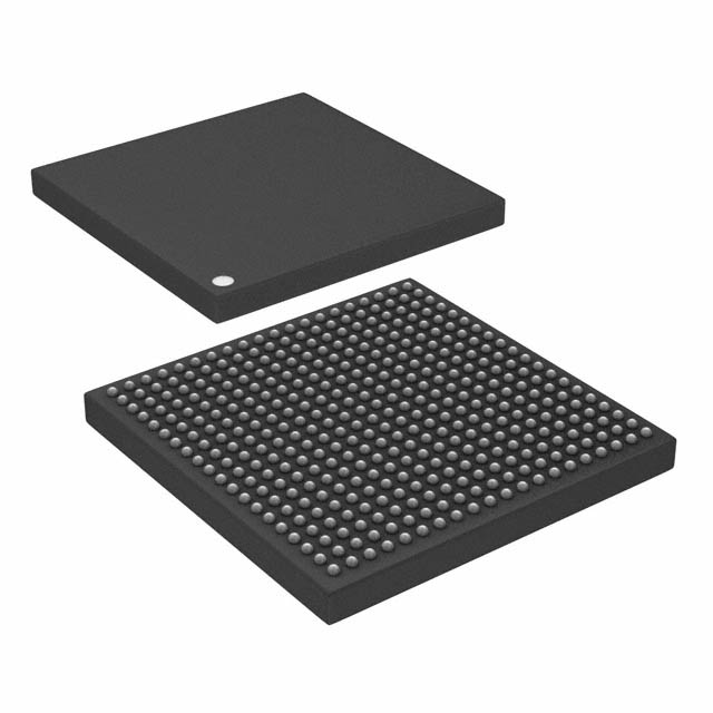
Overview of M2GL010T-FG484 – IGLOO2 FPGA, 12,084 logic elements, 233 I/O, 484‑BGA
The M2GL010T-FG484 is an IGLOO2 flash-based Field Programmable Gate Array from Microchip Technology. Built on the IGLOO2 architecture, it combines low-power flash FPGA fabric with high-performance communications and memory interfaces to address embedded systems, communications, and DSP-oriented designs.
With 12,084 logic elements, approximately 0.9 Mbits of embedded RAM, and 233 user I/Os in a compact 484‑BGA (23×23) package, this device targets designs that require dense logic, substantial on-chip memory, and flexible I/O in a commercial-temperature-rated device.
Key Features
- Flash-based FPGA fabric — IGLOO2 architecture integrates fourth‑generation flash configuration for nonvolatile programmability and low static power.
- Logic capacity — 12,084 logic elements to implement control, glue logic, and mid-density programmable functions.
- On-chip memory — Total of 933,888 bits (approximately 0.9 Mbits) of embedded RAM for buffering, state storage, and small data structures.
- High I/O count — 233 user I/Os supporting multiple voltage standards to interface with sensors, peripherals, and high‑speed PHYs.
- High‑performance communications (series capabilities) — IGLOO2 series supports high‑speed SERDES lanes, XAUI/XGMII extensions, native SERDES, and PCIe endpoint cores for system-level connectivity.
- Memory controller support (series capabilities) — DDRx memory controller options in the IGLOO2 family support LPDDR/DDR2/DDR3 operation and high‑speed external DRAM interfaces.
- DSP and math resources (series capabilities) — Embedded mathblocks and multiplier/accumulator resources in the IGLOO2 architecture enable digital signal processing tasks.
- Clocking resources (series capabilities) — Multiple clock sources and up to eight Clock Conditioning Circuits (CCCs) with integrated PLLs for flexible clocking and phase control.
- Security features (series capabilities) — Design and data security capabilities include encrypted bitstream loading, device certificate models, and optional cryptographic services in premium devices.
- Package and mounting — 484‑BGA (23×23) surface‑mount package optimized for compact board integration.
- Electrical and environmental — Supply voltage range 1.14 V to 2.625 V and commercial operating temperature range 0 °C to 85 °C; RoHS compliant.
Typical Applications
- High‑speed communications — Implement PHY interfaces, PCIe endpoints, and SERDES‑based links using the IGLOO2 communication features in applications such as network appliances and embedded switches.
- Embedded control and interface — Use the device’s 233 I/Os and programmable logic to consolidate sensor interfaces, board control, and protocol bridging in embedded systems.
- Signal processing and DSP — Leverage on‑chip RAM and mathblocks for filtering, accumulation, and other mid‑range DSP tasks in instrumentation and industrial electronics.
- Memory buffering and controller offload — Employ the IGLOO2 memory interfaces and on‑chip RAM to implement data buffering, DDR bridge functions, and memory controller support.
Unique Advantages
- Low‑power, nonvolatile fabric: Flash‑based configuration reduces static power and preserves configuration without external storage.
- Balanced logic and memory: 12,084 logic elements paired with approximately 0.9 Mbits of embedded RAM supports complex control and moderate data buffering on‑chip.
- High I/O density in a compact package: 233 user I/Os in a 484‑BGA (23×23) enable rich external connectivity while conserving PCB area.
- Scalable communications options: Series-level SERDES and PCIe support facilitate integration into networked and high‑throughput system architectures.
- Security and reliability features: IGLOO2 series security mechanisms (encrypted bitstreams, device certificates, anti‑tamper features) help protect IP and supply‑chain integrity.
- Commercial temperature rating and RoHS compliance: Rated 0 °C to 85 °C and RoHS compliant for general commercial applications and standard manufacturing practices.
Why Choose M2GL010T-FG484?
The M2GL010T-FG484 delivers a practical combination of programmable logic density, embedded memory, and flexible I/O in a compact 484‑BGA package. It is suited for designers who need mid‑density FPGA resources with on‑chip RAM and a variety of communication and memory interface options provided by the IGLOO2 architecture.
Its flash‑based configuration, security features, and series‑level support for high‑speed interfaces and memory controllers make it a solid choice for embedded systems, communications equipment, and DSP‑oriented designs where low static power, on‑board nonvolatile configuration, and reliable operation across commercial temperature ranges are required.
Request a quote or submit an inquiry for the M2GL010T-FG484 to receive pricing and availability details or to discuss your application requirements with our team.


Date Founded: 1989
Headquarters: Chandler, Arizona, USA
Employees: 22,000+
Revenue: $8.349 Billion
Certifications and Memberships: ISO9001:2015, IATF16949:2016, AS 9100D


