
JSMC08AUM3HYAEA-H5
| Part Description |
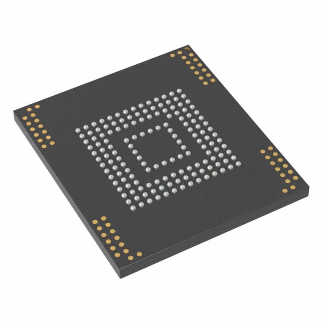
eMMC 5.1, 8GB managed NAND, 240MB/s read, commercial, 153-FBGA |
|---|---|
| Quantity | 886 Available (as of October 7, 2026) |

| Product Category | eMMC Memory |
|---|---|
| Manufacturer | Jeju Semiconductor Corporation |
| Manufacturing Status | Active |
| Manufacturer Standard Lead Time | Contact Us |
| Datasheet |
Specifications & Environmental
| Device Package | 153-BGA (11.5x13mm) | Memory Format | FLASH | Technology | FLASH - NAND (MLC) | ||
|---|---|---|---|---|---|---|---|
| Memory Size | 64 Gbit | Access Time | N/A | Grade | Commercial | ||
| Clock Frequency | 200 MHz | Voltage | 3.3V | Memory Type | Non-Volatile | ||
| Operating Temperature | -25°C - 85°C | Mounting Method | Surface Mount | Memory Interface | eMMC 5.1 | ||
| Memory Organization | N/A | Moisture Sensitivity Level | 3 | RoHS Compliance | Compliant | ||
| REACH Compliance | REACH Unknown | ECCN | EAR99 | HTS Code | 8542.32.00.71 |
Overview of JSMC08AUM3HYAEA-H5 - 8GB eMMC 5.1 Managed NAND 153-FBGA (11.5x13mm)
The JSMC08AUM3HYAEA-H5 doubles capacity to 8GB while keeping the single-die construction and eMMC 5.1 controller of Jeju Semiconductor's managed-NAND line. It draws on one 64Gb die to present 7,818,182,656 bytes of user partition space (LBA 0x00E90000), and the commercial version covers the -25°C to 85°C range. Higher density comes with more headroom on the flash side, and the datasheet reflects that: sustained sequential throughput is rated at 240MB/s read and 55MB/s write, both well above the 4GB member of the family.
Key Features
- 8GB in a single 64Gb die - one NAND die behind the controller yields roughly 7.8GB of user space with no die stacking.
- Faster sustained transfers - 240MB/s sequential read and 55MB/s sequential write, measured under HS400 with cache on, give this density a clear throughput edge over the 4GB part.
- eMMC 5.1 with HS400 - up to 400MB/s bus speed at 200MHz over an 8-bit interface using the 1.8V VCCQ option.
- Dual supply design - VCC flash at 2.7V to 3.6V and VCCQ I/O at 1.70V to 1.95V or 2.7V to 3.6V, with an internal LDO for the NAND rail.
- Enhanced user data area in SLC mode - a configurable region can run in SLC mode for higher-integrity storage, at the cost of double the set-up size.
Typical Applications
- Richer embedded operating systems - 8GB comfortably holds a full Linux or Android stack with room for application data.
- Networking and IoT gateways - the stronger write rate suits devices that log telemetry or buffer traffic locally.
- Digital signage and HMI - media assets and UI resources fit alongside firmware on a single managed device.
Unique Advantages
- Capacity-to-cost balance - a single 64Gb die avoids the expense and thickness of stacked constructions while still doubling 4GB density.
- Write-path improvement - at 55MB/s the rated write speed is more than double the 4GB grade, meaningful for log-heavy and update-heavy workloads.
- Full eMMC 5.1 toolkit - command queuing, cache, Boot and RPMB partitions, Sanitize, Secure Erase and Trim, Field Firmware Update, and a Device Health Report are all present.
Why Choose JSMC08AUM3HYAEA-H5?
The JSMC08AUM3HYAEA-H5 is the right pick when 4GB is tight but a stacked high-capacity device is overkill, and when the design runs in a controlled, commercial-temperature environment. It keeps the same footprint and interface as the smaller grade, so moving up in capacity does not force a board change. Note that Large Sector Size (4KB) is not supported; host formatting should use the standard 512-byte sector, and storage without operation is rated across -40°C to 85°C.
Ask us for a quote on the JSMC08AUM3HYAEA-H5 with up-to-date pricing, stock, and lead time, and tell us your volume so we can lock in availability.




















Date Founded: 2000
Headquarters: Jeju-si, Jeju-do, Republic of Korea
Employees: 100+
Revenue: $100 Million
Certifications and Memberships: ISO9001:2015, ISO14001:2015, AEC-Q100, RoHS, REACH


