
 Selecting between an LDO vs. switching regulator comes down to a trade-off between simplicity/noise and efficiency. LDOs (a type of linear regulator) are quieter and simpler but dissipate more power as heat when the input-to-output voltage difference is large; switching regulators are more efficient but add complexity and switching noise[1].
- LDO: Lower noise/EMI, simpler design, lower efficiency, best for small voltage drops.
- Switching regulator: Higher efficiency, more design complexity, some EMI, best for large voltage drops or higher current.
- Rule of thumb: Use an LDO regulator when there is a small difference between input and output voltage and noise matters; use a switching regulator when efficiency or a large voltage step matters.
Choosing the right topology matters because the wrong one can cause overheating or thermal shutdown, waste board space, or degrade signal integrity. Balancing power dissipation, board space, and noise performance is essential for a stable system architecture.
Key Takeaways
How Linear (LDO) Regulators Work
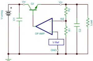
A low dropout regulator (LDO) is a type of linear voltage regulator designed to maintain a stable output voltage even when the input supply voltage is very close to the output voltage[1][5]. LDOs operate continuously in a linear regime, regulating power by dropping excess voltage across an internal pass element.
Basic Architecture — Pass Transistor + Feedback Loop
Typical Use Cases (Low Noise, Low Dropout Needs)
LDOs are the standard choice for powering sensitive analog circuitry where electrical ripple can impair system performance[1]. Common applications include:
- Clocking circuits and low-jitter oscillators.
- High-resolution analog-to-digital converters (ADCs) and sensors.
- Low-power microcontrollers and real-time clocks requiring minimal quiescent current.
- Systems with low voltage differentials, such as regulating a 3.3V rail down to 2.5V (about 76 percent efficient). Larger steps, such as 3.3V to 1.8V (about 55 percent efficient), remain practical at low currents where the dissipated power stays small.
Engineers who need low-noise DC rails with a minimal component count often start with LDO voltage regulators.
How Switching Regulators Work
A switching voltage regulator is an active DC-DC converter that efficiently converts DC input voltages to a regulated DC output using pulse-width modulation (PWM) or pulse-frequency modulation (PFM)[1]. Instead of dissipating excess voltage as heat, switching regulators store energy in reactive components like inductors and capacitors and transfer it in controlled packets each switching cycle, with the output filtered to a smooth DC voltage.
Buck, Boost, & Buck-Boost Basics
Switching regulators are broadly grouped into three primary topologies depending on the relationship between input and output voltage:
- Buck Regulators (Step-Down): Convert a higher input voltage to a lower output voltage[1].
- Boost Regulators (Step-Up): Convert a lower input voltage to a higher output voltage[1].
- Buck-Boost Regulators (Step-Up/Step-Down): Maintain a regulated output voltage whether the input is higher than, lower than, or equal to the output, as in the common non-inverting four-switch buck-boost[1]. A related variant, the inverting buck-boost, produces a negative output rail from a positive input[6].
Typical Use Cases (High Efficiency, Wide Input Range)
Because switchers manage power efficiently, they are used where thermal budgets are tight, or the input voltage range of power supplies varies widely:
- Converting raw battery voltages (e.g., 12V automotive systems) down to 5V or 3.3V logic levels.
- Supplying high-current digital processors, FPGAs, and complex integrated circuits.
- Main supply rails in industrial equipment, telecommunications, and battery-operated IoT nodes.
Designing an efficient buck stage usually involves choosing a power inductor and selecting either a DC-DC converter with integrated switches or a DC-DC controller with external MOSFETs.
Key Differences in Efficiency & Heat: Where Each Topology Wins
Thermal management and energy conservation dictate whether an LDO or a switching converter is appropriate for a given circuit board.
Power Dissipation in LDOs vs. Switchers
The power dissipated by an LDO equals the load current multiplied by the voltage drop across the regulator, plus a small quiescent-current term that is usually negligible[1][3]:
Ploss ≈ (Vin – Vout) × Iout
If an LDO steps down 12V to 3.3V at 1A, it dissipates 8.7W as heat while delivering only 3.3W to the load—yielding an efficiency of roughly 27.5 percent[1].
In contrast, a switching buck converter operates by turning its power switch (internal or external) rapidly ON and OFF. Losses fall into two groups. Conduction losses come from MOSFET on-resistance, the diode drop in non-synchronous designs, and inductor winding resistance. Switching-related losses come from voltage/current overlap during transitions, gate drive, and inductor core loss[1]. A switching regulator under the same 12V to 3.3V at 1A conditions typically yields roughly 85 to 92 percent efficiency, keeping board thermal stress manageable[1].
Efficiency Across Load Conditions
While switching regulators excel under moderate-to-heavy load conditions, their efficiency can degrade at very light loads. Fixed per-cycle losses from switching transitions, gate drive, and inductor core loss, plus quiescent current, become a large share of the small output power[1]. Modern power management ICs often incorporate low-power modes (like PFM) to mitigate this[7]. Conversely, an LDO has no switching losses, so its LDO efficiency stays close to Vout/Vin from light load to full load[1]. Only at very light loads does its quiescent current become a meaningful share of the loss[1][5]. This predictability makes LDOs attractive for standby and always-on rails in battery-powered designs[1].
Parameter LDO (Linear Regulator) Switching Regulator (Buck) Typical Efficiency ≈ Vout/Vin: can exceed 90% with small headroom, below 30% with large drop High (typically 85%–95%+ at moderate-to-heavy load) Noise & Ripple Very low (µV-level output noise) Higher (mV-level ripple plus switching-edge spikes) Board Space & BOM Small (requires input/output caps) Larger (requires inductor and more capacitance; some designs need an external diode or MOSFETs) Thermal Dissipation Scales with (Vin − Vout) × Iout; can be high Low (losses are a small fraction of output power) Design Complexity Low (mostly plug-and-play; check output capacitor stability requirements) Moderate to High (PCB layout sensitive) Step-Up Capability No (step-down only; negative-output LDOs exist for regulating negative rails, but cannot invert polarity) Yes (boost, buck-boost; inverting topologies for negative rails)
For system engineers reviewing power architectures, reading a comprehensive voltage regulator selection guide provides additional context on balancing efficiency against physical board constraints.
Noise & EMI Considerations
RF, clocking, and precision analog circuits depend heavily on clean, low-noise DC power.
Why LDOs Are Quieter
 Because LDOs contain no switching elements, they generate essentially no switching ripple or EMI of their own. Their remaining output noise comes mostly from the internal voltage reference and is typically in the microvolt range
Managing Switching Noise and EMI
Switching regulators toggle current through an inductor at frequencies ranging from hundreds of kilohertz to several megahertz[1]. This rapid switching produces two main types of electrical noise:
- Output Ripple and Conducted Noise: Output voltage ripple at the switching frequency is caused by the inductor’s ripple current flowing through the output capacitor’s capacitance and ESR[1]. Separately, the converter’s pulsating input current creates conducted emissions on the input supply lines[11].
- Radiated EMI: High-frequency electromagnetic radiation caused by fast voltage (dV/dt) and current (dI/dt) transients[11].
Mitigating EMI requires careful layout practices, short current loops, shielding, and dedicated low-pass filtering[11]. In wireless designs, sound antenna placement in PCB design helps keep switching noise from coupling into the RF path.
Cost, Board Space, and BOM Complexity
The economic and practical impact on the bill of materials (BOM) plays a critical role in choosing between LDO and switching regulators.
 LDOs are generally inexpensive and require minimal external components—typically just a small ceramic capacitor at the input and output rails
Decision Framework: When to Use LDO vs. Switching
Use this quick reference framework for LDO vs. switching regulators during schematic capture to select the right regulator for each power rail.
Choose an LDO When:
- The input-to-output voltage differential (Vin − Vout) is very small[8].
- Output current is low enough that the dissipated power, (Vin − Vout) × Iout, stays within the package’s thermal limits. LDOs are available at 1A and above, but with larger voltage drops even a few hundred milliamps can overheat a small package[1][3].
- The application demands ultra-low noise, high PSRR, and zero switching ripple.
- PCB real estate is constrained and cannot accommodate a power inductor.
- Low initial BOM cost and short design cycles are primary drivers.
Choose a Switching Regulator When:
- Stepping down a high input voltage to a much lower output rail at high currents and high power.
- Efficiency is paramount, such as in battery-operated or thermally constrained enclosures[1].
- The application requires stepping up a voltage (Boost) or output polarity inversion[1][6].
- Total power dissipation of an equivalent LDO would exceed thermal limits[1].
System designers working through complex architectures can leverage engineering design support to validate power budgets early in the hardware cycle.
Hybrid Approaches: Using Both in One Design
In modern system architectures, engineers frequently combine both linear and switching topologies into a hybrid regulation scheme to capture the benefits of both worlds.
In a hybrid configuration, a switching buck regulator efficiently steps down a high system voltage (e.g., 12V or 24V) to an intermediate rail slightly above the final target voltage. It needs enough headroom to cover the LDO’s worst-case dropout plus margin for ripple rejection (e.g., roughly 3.6V to 3.8V for a 3.3V output)[2][4]. An LDO then regulates that intermediate rail down to the final target voltage, and a power good signal can indicate when each stage is in regulation.
This cascading approach keeps most of the buck converter’s power efficiency. For example, a 90 percent-efficient buck feeding a 3.6V-to-3.3V LDO (about 92 percent efficient) delivers roughly 83 percent overall, versus 27.5 percent for a single LDO stepping 12V directly to 3.3V. The LDO then attenuates the remaining switching ripple and delivers a quieter rail to sensitive loads such as data converters, PLLs, and high-speed clocks. Because LDO ripple rejection is strongest at lower frequencies, a ferrite bead or LC filter is often added to suppress higher-frequency switching harmonics[4].
When finalizing power tree selections or sourcing alternatives, review general guidelines on innovations in power management ICs, look at power sequencing ICs for multi-rail startup control, or contact the technical team at Suntsu.
Sourcing LDO and Switching Regulators
The right topology only helps if the parts are available when production starts. Suntsu supplies both LDOs and switching regulators from manufacturers including:


Need Support Optimizing Your Power Architecture?
Navigating the trade-offs between efficiency, board space, and noise performance requires balancing both engineering requirements and component availability. Suntsu offers a comprehensive portfolio of power management ICs, LDO regulator ICs, DC-DC controllers, and power inductors to keep your designs running on reliable power.
Whether you need assistance selecting drop-in alternatives for obsolete power parts or want a comprehensive BOM review, our engineering team is here to help. Get a Quote or Contact Us today to connect with an application specialist.
FAQs
Start with the LDO’s power dissipation, PD ≈ (Vin − Vout) × Iout + Vin × Iground. Then estimate junction temperature with TJ = TA + (PD × RθJA), where RθJA is the junction-to-ambient thermal resistance from the datasheet[3][12]. Package choice matters a great deal. For example, the TPS732 is rated at 205.9°C/W in a SOT-23 package but 53.1°C/W in a SOT-223, so the same 5.5V-to-3V, 250mA load produces a junction temperature of about 155°C in the SOT-23 versus under 60°C in the SOT-223 at 25°C ambient[12]. Most LDOs enter thermal shutdown around 160°C, so the target should be the datasheet’s recommended operating junction temperature (often 125°C) with margin. Also keep in mind that datasheet RθJA values are measured on a standard JEDEC test board. Larger copper planes for VIN, VOUT, and ground lower the real-world thermal resistance[12].
Dropout is set mostly by the pass transistor’s architecture and its on-resistance at a given load current[5][13]. In a PMOS LDO, the gate is pulled toward ground to turn the device on, so the gate-source voltage grows with input voltage. This is why PMOS architectures have lower dropout at higher output voltages[13]. An NMOS pass device has lower on-resistance per unit area, but its gate must be driven above the output voltage, which the input rail alone can’t always provide at low output voltages. Many NMOS LDOs therefore use an auxiliary bias rail that powers the error amplifier and lets its output swing above VIN, enabling ultra-low dropout at low output voltages. Others use an internal charge pump instead[13]. Dropout is not a fixed value, either: it rises with load current and temperature, so check the dropout curves at your worst-case operating point.
The output capacitor is part of the LDO’s feedback loop. Its equivalent series resistance (ESR) creates a zero in the loop response at f = 1 / (2π × ESR × Cout), which provides phase boost needed for stability[14]. If ESR is too low, the zero moves too high in frequency to help. If ESR is too high, it adds gain at high frequencies and can also cause instability. Choosing an output capacitor for LDOs with PNP or PMOS pass elements can be difficult because of these specific ESR requirements, and older devices were designed around tantalum capacitors with ESR in a defined window[14]. Most modern LDOs are internally compensated to be stable with low-ESR ceramics. Even so, designers should confirm the minimum effective capacitance after accounting for DC bias derating of ceramic capacitors, and verify stability with a load-step test on the actual board.
Switching frequency is a trade-off between size and efficiency. A higher frequency allows smaller inductors and capacitors, but switching-related losses (transition overlap, gate drive, and core loss) scale with frequency[1]. Frequency placement also matters for EMI[11]. In automotive designs, a clean approach is to set the switching frequency above the top of the AM radio band at 1.8MHz, which is why 2MHz-class converters are common in those applications[15]. Similar thinking applies to any system with sensitive bands, such as keeping the switching frequency and its harmonics away from an ADC’s signal band or an RF channel. At high step-down ratios, high frequencies may also be limited by the converter’s minimum on-time[15][16].
In a non-synchronous buck, the catch diode conducts during the entire off-time, so its forward voltage drop (typically 0.3V to 0.5V for a Schottky) becomes a major loss at low output voltages and low duty cycles[1]. Converting 12V to 1.2V, for example, means the diode conducts about 90 percent of each cycle, and a 0.4V drop is a third of the output voltage. A synchronous buck replaces the diode with a low-side MOSFET whose on-resistance drop is much smaller[1][17]. However, synchronous buck converters are not always more efficient. At light loads, a non-synchronous design can be more efficient, and at higher output voltages the diode’s loss is a smaller share of the output power[17]. Non-synchronous designs can also make sense for cost, simplicity, or very high input voltages.
Related Content
References
- H. Zhang. “AN-140: Basic Concepts of Linear Regulator and Switching Mode Power Supplies” Available at: https://www.analog.com/en/resources/app-notes/an-140.html
- G. Morita. “Ask the Applications Engineer—41: LDO Operational Corners: Low Headroom and Minimum Load” Available at: https://www.analog.com/en/resources/analog-dialogue/articles/ldo-operational-corners.html
- B. Hunter and P. Rowland. “Linear Regulator Design Guide For LDOs” Available at: https://www.ti.com/lit/an/slva118/slva118.pdf
- K. Shimo, I. Ardiente, and A. Limjoco. “Optimizing LDO Headroom Control with a Current Reference Switching Regulator Design—Part 1: Noise Sources, Impact, and Strategies” Available at: https://www.analog.com/en/resources/technical-articles/optimizing-ldo-headroom-control-part-1.html
- B. Lee. “Understanding the Terms and Definitions of LDO Voltage Regulators” Available at: https://www.ti.com/lit/an/slva079/slva079.pdf
- F. De Stasi. “Working With Inverting Buck-Boost Converters” Available at: https://www.ti.com/lit/snva856
- S. Jaffe and K. Wiggenhorn. “Understanding Mode Transitions for LMR33620/30 and LMR36006/15” Available at: https://www.ti.com/lit/pdf/snva857
- T. Gross. “LDO Linear Regulators Rival Switchers for Efficiency” Available at: https://www.analog.com/en/resources/technical-articles/ldo-linear-regulators-rival-switchers-efficiency.html
- G. Morita. “AN-1120: Noise Sources in Low Dropout (LDO) Regulators” Available at: https://www.analog.com/en/resources/app-notes/an-1120.html
- A. Paxton. “LDO Basics: Power Supply Rejection Ratio” Available at: https://www.ti.com/lit/pdf/ssztad7
- Texas Instruments. “AN-2155LayoutTipsforEMIReductioninDC/DC Converters” Available at: https://www.ti.com/lit/an/snva638a/snva638a.pdfl
- W. Fwu. “LDO Basics: Thermals – How Hot Is Your Application?” Available at: https://www.ti.com/lit/pdf/sszt950l
- A. Paxton. “LDO Basics: Dropout” Available at: https://www.ti.com/lit/pdf/ssztac2
- J. Falin. “ESR, Stability, and the LDO Regulator” Available at: https://www.ti.com/lit/an/slva115/slva115.pdf
- P. Wong. “2MHz Dual Buck Regulator Operates Outside of AM Radio Band When Delivering 3.3V and 1.8V from 16V Input” Available at: https://www.analog.com/en/resources/technical-articles/2mhz-dual-buck-regulator-operates-outside-of-am-radio-band.html
- D. Tseng. “How to Overcome Minimum On-time Challenges in Switching Power Supplies” Available at: https://www.ti.com/lit/pdf/ssztah4
- R. Nowakowski and N. Tang. “Efficiency of synchronous versus nonsynchronous buck converters” Available at: https://www.ti.com/lit/pdf/slyt358