W25N512GVEIG TR
| Part Description |
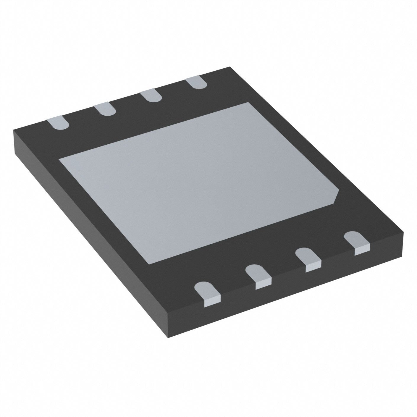
IC FLASH 512MBIT SPI/QUAD 8WSON |
|---|---|
| Quantity | 696 Available (as of June 15, 2026) |

| Product Category | Flash Memory |
|---|---|
| Manufacturer | Winbond Electronics |
| Manufacturing Status | Active |
| Manufacturer Standard Lead Time | 24 Weeks |
| Datasheet |
Specifications & Environmental
| Device Package | 8-WSON (8x6) | Memory Format | FLASH | Technology | FLASH - NAND (SLC) | ||
|---|---|---|---|---|---|---|---|
| Memory Size | 512 Mbit | Access Time | 6 ns | Grade | Industrial | ||
| Clock Frequency | 166 MHz | Voltage | 2.7V ~ 3.6V | Memory Type | Non-Volatile | ||
| Operating Temperature | -40°C ~ 85°C (TA) | Write Cycle Time Word Page | 700 μs | Packaging | 8-WDFN Exposed Pad | ||
| Mounting Method | Non-Volatile | Memory Interface | SPI - Quad I/O | Memory Organization | 64M x 8 | ||
| Moisture Sensitivity Level | 3 (168 Hours) | RoHS Compliance | ROHS3 Compliant | REACH Compliance | REACH Unaffected | ||
| Qualification | N/A | ECCN | 3A991B1A | HTS Code | 8542.32.0071 |
Overview of W25N512GVEIG TR – IC FLASH 512MBIT SPI/QUAD 8WSON
The W25N512GVEIG TR is a 3V, 512 M-bit serial SLC NAND flash memory device implementing Dual/Quad SPI with buffer read and continuous read modes. It provides non-volatile, byte-addressable storage organized as 64M x 8 and is intended for systems that require serial flash storage accessible via SPI or Quad I/O.
With a 2.7 V to 3.6 V supply range, support for standard/dual/quad SPI instructions, and on-die protection and configuration registers, the device targets designs needing robust serial flash functions including read, program and erase operations at a 166 MHz clock capability.
Key Features
- Memory Type & Capacity 512 Mbit SLC NAND flash organized as 64M x 8 for non-volatile data and code storage.
- Interface SPI — Quad I/O support with Dual/Quad SPI instructions and standard SPI compatibility for flexible host interfacing.
- Read Modes Buffer Read and Continuous Read modes are supported to optimize sequential data transfers.
- Performance Device supports up to 166 MHz clock frequency with an access time specified at 6 ns for read operations.
- Program/Erase Timing Write cycle time (word/page) specified at 700 µs; instruction set includes page program, quad load program, and 128KB block erase commands.
- Voltage & Temperature Range Operates from 2.7 V to 3.6 V and is specified for an ambient temperature range of −40 °C to 85 °C.
- Protection & Configuration Volatile writable protection and configuration registers with OTP-lockable bits (block protect, WP-E, SRP bits), ECC enable bit, and status registers for program/erase and ECC reporting.
- Package Available in an 8-WSON (8x6) exposed pad package (8-WDFN style) for compact PCB footprint and thermal/power handling.
Typical Applications
- Non-volatile storage — 512 Mbit serial SLC NAND FLASH provides storage for system data and assets accessible via SPI/Quad I/O.
- Boot and code shadowing — Dual/Quad SPI and buffer/continuous read modes enable serial execution and fast code retrieval where supported.
- Data logging and file storage — Page program and block erase commands allow managed write/erase cycles for recorded data storage.
Unique Advantages
- Serial SLC NAND in a compact package: 512 Mbit capacity in an 8-WSON (8x6) package reduces PCB area while providing high-density non-volatile storage.
- Flexible SPI performance: Dual and Quad SPI support plus buffer/continuous read modes enable higher-throughput serial transfers when required.
- Wide operating range: 2.7 V to 3.6 V supply and −40 °C to 85 °C ambient rating accommodate a range of host systems and environments.
- Configurable protection and ECC: Protection and configuration registers include OTP-lockable bits and an ECC enable option with cumulative ECC status reporting for managed data integrity.
- Comprehensive instruction set: Includes device reset, JEDEC ID, read, program (including quad load program), and 128KB block erase commands for full flash management.
Why Choose IC FLASH 512MBIT SPI/QUAD 8WSON?
The W25N512GVEIG TR delivers a verified 512 Mbit SLC NAND flash solution with Dual/Quad SPI connectivity, buffer and continuous read modes, and on-chip protection/configuration controls. Its combination of serial interface flexibility, 166 MHz clock capability, and SLC NAND organization makes it suitable for system designs that require compact, non-volatile storage with configurable protection and ECC support.
This device is well suited to designers looking for a high-density, SPI-accessible flash memory in a small 8-WSON package and for applications that require documented instruction support for read, program and erase operations along with writable and OTP-lockable protection registers.
Request a quote or submit an inquiry for pricing, availability and lead-time information to proceed with evaluation or volume sourcing of the W25N512GVEIG TR.