W25N512GVEIG
| Part Description |
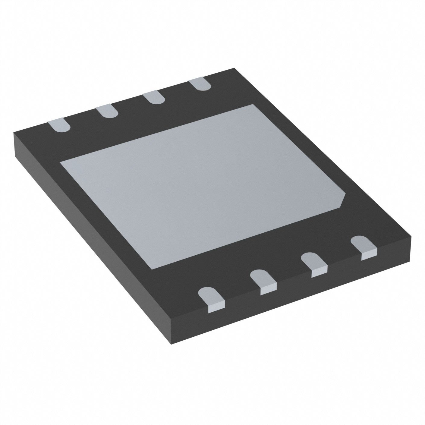
IC FLASH 512MBIT SPI/QUAD 8WSON |
|---|---|
| Quantity | 796 Available (as of June 15, 2026) |

| Product Category | Flash Memory |
|---|---|
| Manufacturer | Winbond Electronics |
| Manufacturing Status | Active |
| Manufacturer Standard Lead Time | 24 Weeks |
| Datasheet |
Specifications & Environmental
| Device Package | 8-WSON (8x6) | Memory Format | FLASH | Technology | FLASH - NAND (SLC) | ||
|---|---|---|---|---|---|---|---|
| Memory Size | 512 Mbit | Access Time | N/A | Grade | Industrial | ||
| Clock Frequency | 166 MHz | Voltage | 2.7V ~ 3.6V | Memory Type | Non-Volatile | ||
| Operating Temperature | -40°C ~ 85°C (TA) | Write Cycle Time Word Page | 700 μs | Packaging | 8-WDFN Exposed Pad | ||
| Mounting Method | Non-Volatile | Memory Interface | SPI - Quad I/O | Memory Organization | 64M x 8 | ||
| Moisture Sensitivity Level | 3 (168 Hours) | RoHS Compliance | ROHS Compliant | REACH Compliance | REACH Unaffected | ||
| Qualification | N/A | ECCN | 3A991B1A | HTS Code | 8542.32.0071 |
Overview of W25N512GVEIG – IC FLASH 512MBIT SPI/QUAD 8WSON
The W25N512GVEIG is a 3.0 V, 512 Mbit serial SLC NAND flash memory organized as 64M x 8 and designed for SPI/Quad I/O access. It implements Dual/Quad SPI with buffer read and continuous read modes, providing a serial non-volatile storage option for embedded systems requiring moderate-density flash.
This device targets designs that need a 512 Mbit SLC NAND memory with a serial SPI interface, supporting operation from 2.7 V to 3.6 V and an ambient temperature range of -40°C to 85°C.
Key Features
- Memory Type & Capacity — 512 Mbit SLC NAND flash, organized as 64M × 8 for byte-wide access.
- Serial Interface — SPI with Dual and Quad I/O support for higher throughput and flexible read modes including buffer read and continuous read.
- Clock Rate — Supports operation up to 166 MHz clock frequency for high-speed serial transfers.
- Voltage and Power — Single supply operation from 2.7 V to 3.6 V to suit 3V system rails.
- Program/Erase and Timing — Page/word program write cycle time specified at 700 µs (word/page program).
- Protection & Management — On-chip protection, configuration and status registers including block protection bits, OTP lockable bits, ECC status and bad block management as described in the device instruction set.
- Package Options — Available in an exposed-pad 8-WDFN and in an 8-WSON (8×6) package format for compact board integration.
- Operating Temperature — Industrial temperature range: -40°C to 85°C (TA).
Typical Applications
- Embedded Storage — Serial non-volatile storage for firmware, code and data in embedded systems that require SPI/Quad I/O flash.
- Consumer & Industrial Electronics — On-board flash memory for devices operating within a −40°C to 85°C ambient range and a 2.7–3.6 V supply.
- Data Logging and Buffering — Buffer read and continuous read modes support sequential data retrieval for logging applications.
Unique Advantages
- 512 Mbit SLC NAND Density: Provides high-density non-volatile storage in a compact serial package for designs that need 64M × 8 organization.
- Flexible High-Speed SPI I/O: Dual/Quad SPI with up to 166 MHz clocking and buffer/continuous read modes enables higher effective throughput over the serial bus.
- System Voltage Compatibility: 2.7 V–3.6 V supply range aligns with common 3V system rails simplifying power-domain design.
- On-Chip Management and Protection: Built-in protection, configuration and status registers (including OTP lockable bits and ECC status indicators) support reliable data management and control.
- Compact Package Choices: Available in exposed-pad 8-WDFN and 8-WSON (8×6) packages to support compact PCB layouts and thermal considerations.
- Industrial Temperature Range: Rated for -40°C to 85°C ambient operation to cover a wide range of deployed environments.
Why Choose W25N512GVEIG?
The W25N512GVEIG combines 512 Mbit SLC NAND density with a serial Dual/Quad SPI interface, buffer read and continuous read modes to deliver a compact, high-density non-volatile memory option for embedded designs. Its supported clock rate, on-chip protection and configuration registers, and specified program timing make it suitable for systems that require controlled program/erase management and serial access.
This device is suited to designers and procurement teams specifying a 3V SLC NAND flash with SPI/Quad I/O, compact package options, and an industrial operating temperature range. The documented registers and instruction set support integration into systems that need explicit control over protection, ECC status and bad block management.
Request a quote or submit an inquiry for pricing and availability to obtain lead-time and ordering information for the W25N512GVEIG serial SLC NAND flash device.