
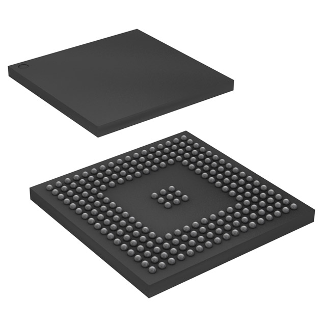
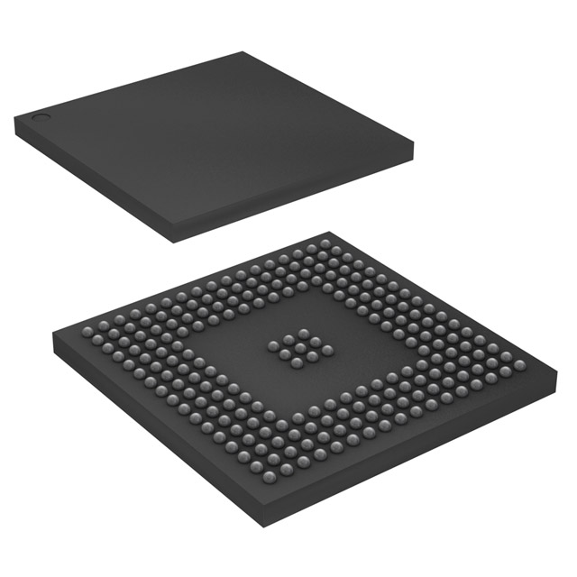
AT91SAM9CN11-CU
| Part Description |
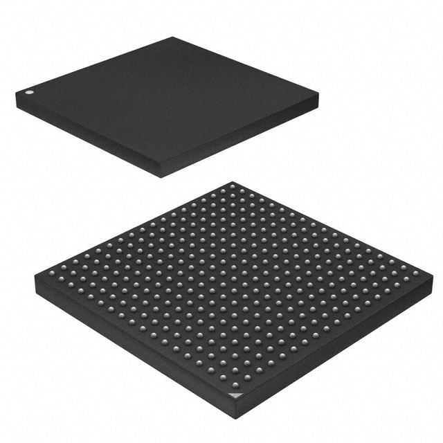
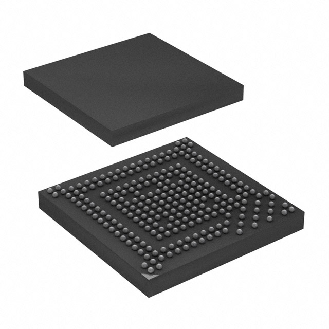
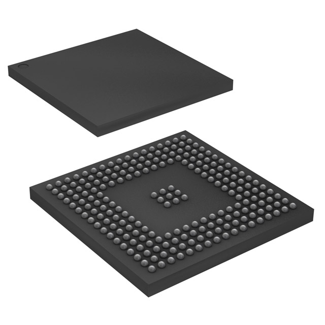
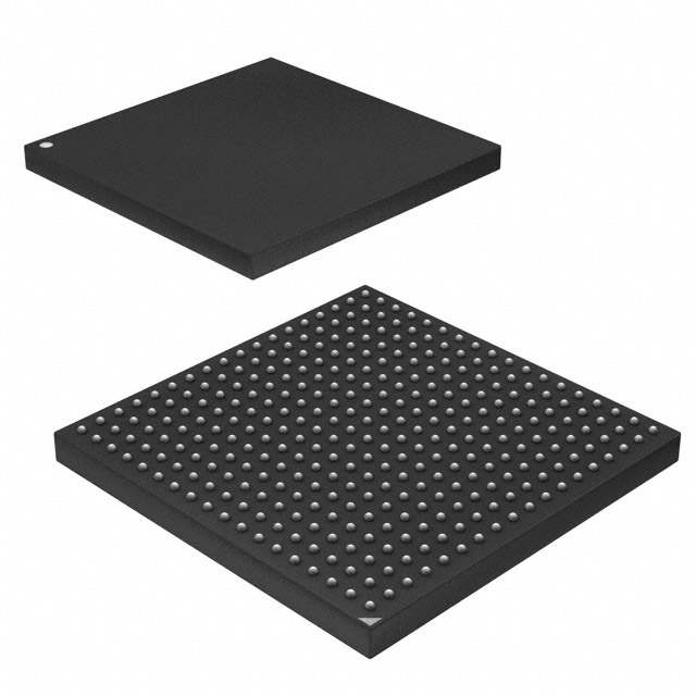
ARM926EJ-S Microprocessor IC SAM9CN 1 Core, 32-Bit 400MHz 217-LFBGA (15x15) |
|---|---|
| Quantity | 234 Available (as of October 8, 2026) |
| Product Category | Microprocessors |
|---|---|
| Part Series | SAM9CN |
| Manufacturer | Microchip Technology |
| Manufacturing Status | Active |
| Manufacturer Standard Lead Time | 52 Weeks |
| Datasheet |
Specifications & Environmental
| Core Processor | ARM926EJ-S | Device Package | 217-LFBGA (15x15) | Display & Interface Controllers | LCD, Touchscreen | ||
|---|---|---|---|---|---|---|---|
| ECCN | 5A002A1 ATM | Grade | Industrial | Graphics Acceleration | No | ||
| HTS Code | 8542.31.0001 | Moisture Sensitivity Level | 3 (168 Hours) | Mounting Method | Surface Mount | ||
| Mounting Type | Surface Mount | Number of Cores/Bus Width | 1 Core, 32-Bit | Operating Temperature | -40°C ~ 85°C (TA) | ||
| Package / Case | 217-LFBGA | RAM Controllers | LPDDR, LPDDR2, DDR2, SDR, SRAM | REACH Compliance | REACH Unaffected | ||
| RoHS Compliance | ROHS3 Compliant | Speed | 400MHz | Supplier Device Package | 217-LFBGA (15×15) | ||
| USB | USB 2.0 (2) | Voltage – I/O | 1.8V, 3.3V |
Overview of AT91SAM9CN11-CU – IC MPU SAM9CN 400MHZ 217LFBGA
The AT91SAM9CN11-CU is a 32-bit embedded microprocessor based on the ARM926EJ-S core, running at 400 MHz in a single-core configuration. Designed for embedded and industrial applications, it combines processing performance with rich connectivity, memory and user-interface support for systems requiring LCD/touchscreen display control, USB connectivity and high-speed memory interfaces.
This device delivers an integrated platform-level feature set—including support for LPDDR/DDR2 and NAND, USB Host and Device, advanced security accelerators and a multi-layer bus with DMA—to simplify system design and accelerate time to market in industrial and embedded designs.
Key Features
- Core ARM926EJ-S 32-bit processor running up to 400 MHz with instruction and data caches and an MMU for embedded OS support.
- Memory Interfaces External memory support for LPDDR, LPDDR2, DDR2, SDR and SRAM plus an external bus interface supporting 8-bank DDR2/LPDDR and static memories; on-chip 128 KB ROM and 32 KB SRAM are included in the architecture.
- Display and HMI Integrated LCD controller and resistive touchscreen support for user-interface applications.
- Connectivity Two USB 2.0 full-speed interfaces (Host and Device), SDIO and multiple UART/SPI/I²C peripherals for broad I/O connectivity.
- Security and Acceleration On-chip hardware accelerators supporting up to 256-bit AES and FIPS 180-2 compliant SHA1/SHA256, plus a True Random Number Generator (TRNG) and fuse bits for user and device configuration.
- System and DMA 133 MHz multi-layer AHB bus architecture with dual peripheral bridge and an 8-channel dual-port DMA controller to sustain high peripheral and memory throughput.
- Power and Clocks Integrated power-on reset, reset and shutdown controllers, watchdog, RTC, internal low-power 32 kHz RC and fast 12 MHz RC oscillators, plus PLLs for system and USB clocking.
- Package and Temperature 217-ball LFBGA (15×15) surface-mount package; industrial operating temperature range −40 °C to 85 °C.
- Peripheral Storage Support MLC/SLC NAND controller with programmable multi-bit ECC (PMECC) for robust flash storage implementations.
Typical Applications
- Industrial HMI and Control Panels Use the integrated LCD controller and touchscreen support to implement user interfaces while leveraging industrial temperature rating for harsh environments.
- Embedded Connectivity Gateways USB Host/Device, SDIO and multiple serial interfaces enable gateway designs that bridge sensors, storage and host systems.
- Secure Embedded Storage and Authentication Hardware AES/SHA accelerators and TRNG support secure boot, encryption and authentication for devices handling sensitive data.
- Multimedia and Display Systems The processor and memory interface support enable display-driven embedded applications requiring responsive UI and data throughput.
Unique Advantages
- Single-chip integration: Combines CPU, memory controllers, display and USB peripherals to reduce BOM and simplify board design.
- High data-path throughput: Multi-layer AHB bus with 8-channel DMA sustains data movement between peripherals and external memory without overloading the CPU core.
- Security primitives on-chip: AES and SHA accelerators plus a TRNG and configurable fuse bits facilitate secure storage and communications designs.
- Flexible memory support: Native support for LPDDR/DDR2/SDR and NAND expands choices for performance and cost-optimized memory architectures.
- Industrial-grade operation: Specified −40 °C to 85 °C and available in a compact 217-LFBGA package suitable for space-constrained, ruggedized products.
Why Choose AT91SAM9CN11-CU?
The AT91SAM9CN11-CU positions itself as a versatile embedded MPU that balances up to 400 MHz ARM926EJ-S processing performance with an extensive set of on-chip peripherals and memory interfaces. Its integrated security accelerators, DMA-capable system bus and dedicated display and USB controllers make it well suited for industrial HMI, secure storage and connectivity-focused designs.
This device is targeted at engineers and product teams building industrial and embedded systems that require sustained data throughput, on-chip security features and flexible memory connectivity, while keeping board complexity and component count under control.
Request a quote or submit an inquiry to get pricing, lead-time and ordering information for the AT91SAM9CN11-CU.






















Date Founded: 1989
Headquarters: Chandler, Arizona, USA
Employees: 22,000+
Revenue: $8.349 Billion
Certifications and Memberships: ISO9001:2015, IATF16949:2016, AS 9100D




