
ATSAMA5D31A-CFUR
| Part Description |
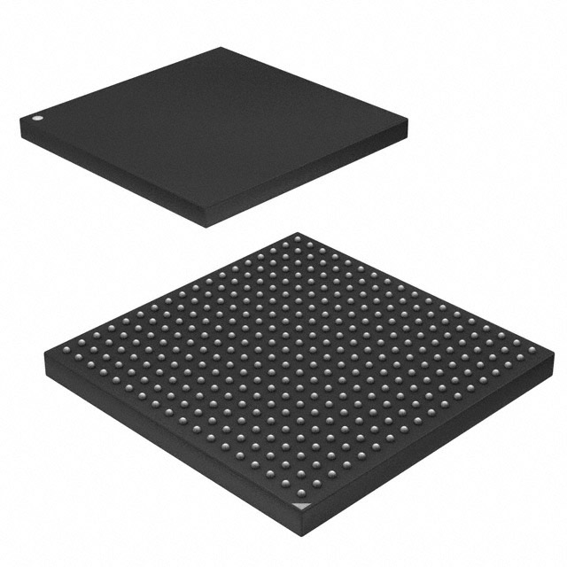
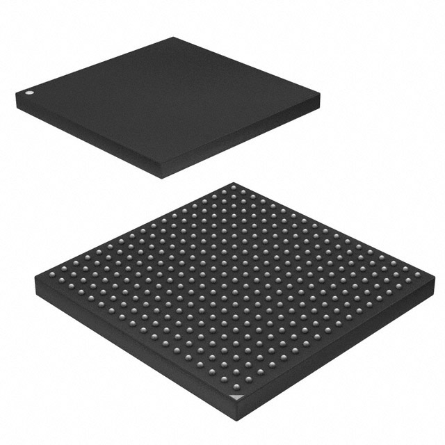
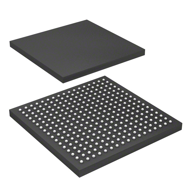
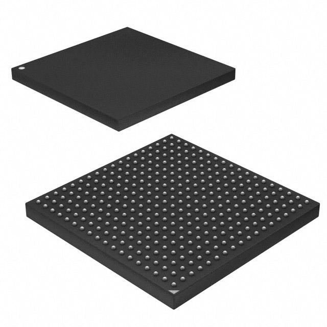
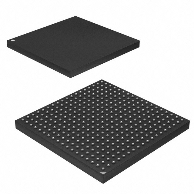
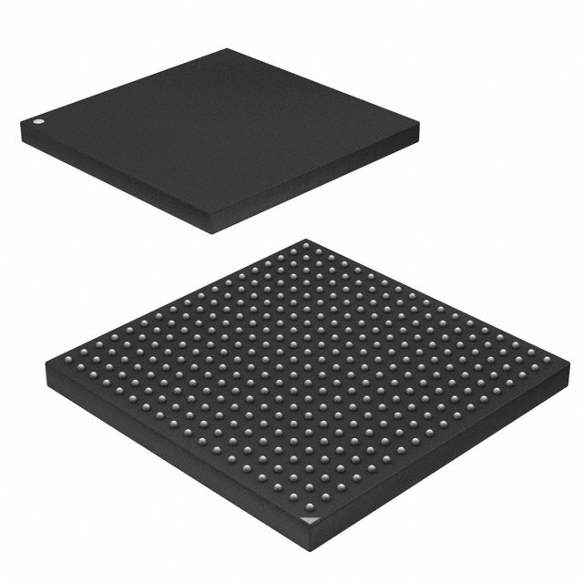
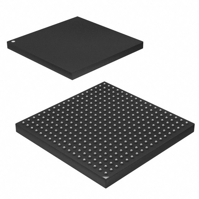
ARM® Cortex®-A5 Microprocessor IC SAMA5D3 1 Core, 32-Bit 536MHz 324-TFBGA (15x15) |
|---|---|
| Quantity | 344 Available (as of October 8, 2026) |
| Product Category | Microprocessors |
|---|---|
| Part Series | SAMA5D3 |
| Manufacturer | Microchip Technology |
| Manufacturing Status | Active |
| Manufacturer Standard Lead Time | 7 Weeks |
| Datasheet |
Specifications & Environmental
| Core Processor | ARM® Cortex®-A5 | Device Package | 324-TFBGA (15x15) | Display & Interface Controllers | LCD, Touchscreen | ||
|---|---|---|---|---|---|---|---|
| ECCN | 5A992C | Ethernet | 10/100Mbps (1) | Grade | Industrial | ||
| Graphics Acceleration | No | HTS Code | 8542.31.0001 | Moisture Sensitivity Level | 3 (168 Hours) | ||
| Mounting Method | Surface Mount | Mounting Type | Surface Mount | Number of Cores/Bus Width | 1 Core, 32-Bit | ||
| Operating Temperature | -40°C ~ 85°C (TA) | Package / Case | 324-TFBGA | RAM Controllers | LPDDR, LPDDR2, DDR2 | ||
| REACH Compliance | REACH Unaffected | RoHS Compliance | ROHS3 Compliant | Security Features | AES, SHA, TDES, TRNG | ||
| Speed | 536MHz | Supplier Device Package | 324-TFBGA (15×15) | USB | USB 2.0 (3) | ||
| Voltage – I/O | 1.2V, 1.8V, 3.3V |
Overview of ATSAMA5D31A-CFUR – IC MPU SAMA5D3 536MHz 324TFBGA
The ATSAMA5D31A-CFUR is an ARM® Cortex®-A5 based microprocessor IC from Microchip Technology’s SAMA5D3 series, running at up to 536 MHz. It combines a single 32-bit Cortex‑A5 core with a floating point unit and a high-bandwidth multi-layer bus to deliver efficient processing for connected embedded systems.
Designed for industrial-grade applications, this device targets user interfaces, industrial connectivity and secure embedded systems by offering integrated memory controllers, extensive peripheral support and hardware security acceleration.
Key Features
- Core and Performance ARM® Cortex®-A5 core at up to 536 MHz with an integrated floating point unit (VFPv4), 32 KB instruction and 32 KB data caches, and a fully integrated MMU for efficient application execution.
- Memory Subsystem Internal memory includes a 160 Kbyte ROM and 128 Kbyte SRAM. High-bandwidth 32-bit multi-port DRAM controller supports DDR2/LPDDR/LPDDR2 up to 512 Mbyte with datapath scrambling; independent static memory controller with NAND support and up to 24-bit ECC.
- Connectivity & Peripherals Multiple mainstream interfaces including 10/100 Mbps Ethernet, Gigabit EMAC support and IEEE1588 (per datasheet), three USB 2.0 ports, CAN, UART, SPI and I2C for broad I/O and networking options.
- Display & Imaging Integrated LCD controller with overlays and a touchscreen interface plus a CMOS sensor interface to support rich human‑machine interfaces and image capture.
- Security Hardware-accelerated cryptography including AES, SHA, TDES and a True Random Number Generator (TRNG) plus secure boot features to protect code and external data transfers.
- System Services & DMA High data throughput is enabled by a multi-layer bus architecture and 39 DMA channels, plus advanced interrupt control and programmable fuse bits for configuration and protection.
- Low Power & Power Management Multiple low-power modes and a power management controller deliver sub-milliwatt consumption in low-power mode (below 0.5 mW as described in the datasheet), suitable for energy-conscious designs.
- Package & Environmental 324‑TFBGA surface-mount package (15 × 15 mm) rated for industrial operating temperatures from −40 °C to 85 °C and RoHS compliant.
Typical Applications
- Industrial HMI and Control Panels Drive touchscreen displays and complex UI overlays while handling connectivity to field networks and sensors.
- Secure Embedded Gateways Aggregate and secure data using onboard Ethernet, USB and hardware crypto engines for protected communications and storage.
- Portable and Battery‑Aware Devices Low-power modes and efficient processing make it suitable for battery-operated products that require responsive user interfaces.
- Imaging and Sensor Interfaces Use the CMOS sensor interface and LCD controller to support camera input and real-time display tasks in embedded vision applications.
Unique Advantages
- Single-chip integration: Core, memory controllers, display and rich peripheral set reduce BOM and simplify board-level design.
- Hardware security acceleration: AES, SHA, TDES and TRNG provide on-chip cryptographic performance for secure boot and trusted data handling.
- High-throughput architecture: Multi-layer bus with 39 DMA channels and advanced interrupt control sustains demanding data flows between peripherals and memory.
- Memory flexibility: Support for DDR2/LPDDR/LPDDR2 and multi-level NAND with 24-bit ECC enables scalable storage and RAM choices for varied application needs.
- Industrial temperature range: −40 °C to 85 °C rating supports deployment in robust, field-facing equipment.
- Compact surface-mount package: 324‑TFBGA (15×15 mm) balances integration density with manufacturability for production designs.
Why Choose ATSAMA5D31A-CFUR?
The ATSAMA5D31A-CFUR positions itself as a versatile, industrial-grade MPU combining a capable Cortex‑A5 core, hardware floating point acceleration and a comprehensive set of connectivity and security features. Its high-bandwidth memory architecture and DMA resources make it well suited for applications that require responsive user interfaces, secure communications and sustained peripheral data transfer.
This part is appropriate for design teams and OEMs building industrial HMIs, secure gateways, imaging-enabled products and low-power embedded systems that demand integration, long-term robustness and a clear upgrade path within the SAMA5D3 series.
Request a quote or submit an RFQ for the ATSAMA5D31A-CFUR using the part number to begin procurement or to obtain pricing and availability information.






















Date Founded: 1989
Headquarters: Chandler, Arizona, USA
Employees: 22,000+
Revenue: $8.349 Billion
Certifications and Memberships: ISO9001:2015, IATF16949:2016, AS 9100D




