
LS1046AXE8Q1A
| Part Description |
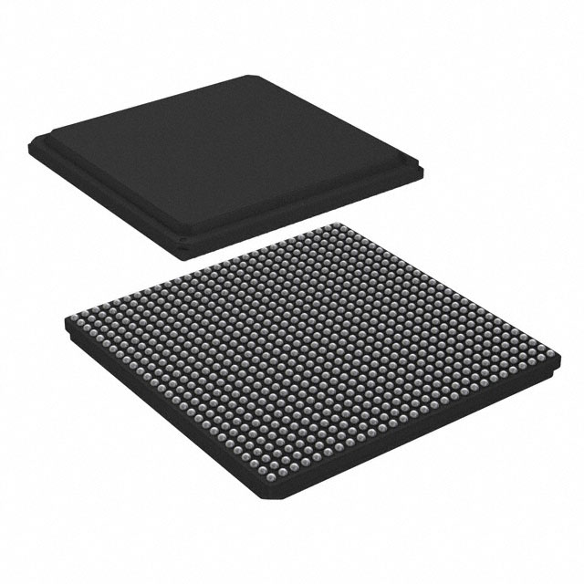
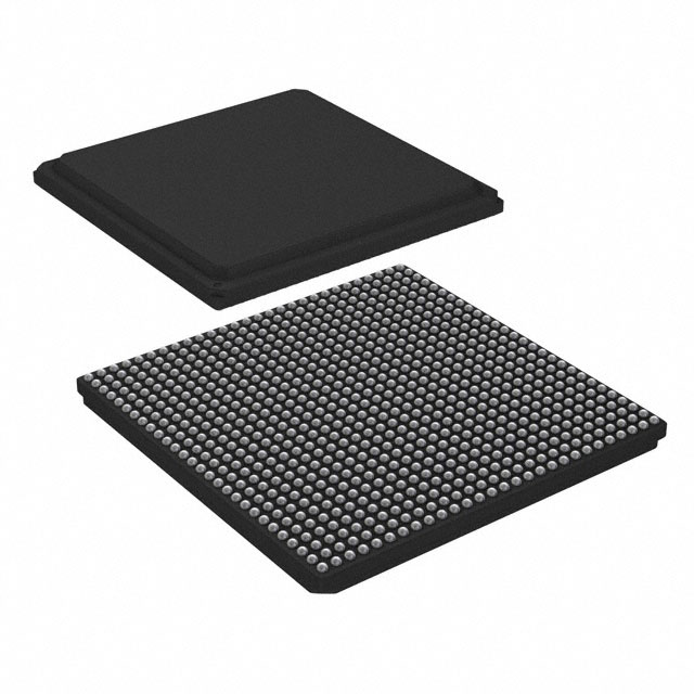
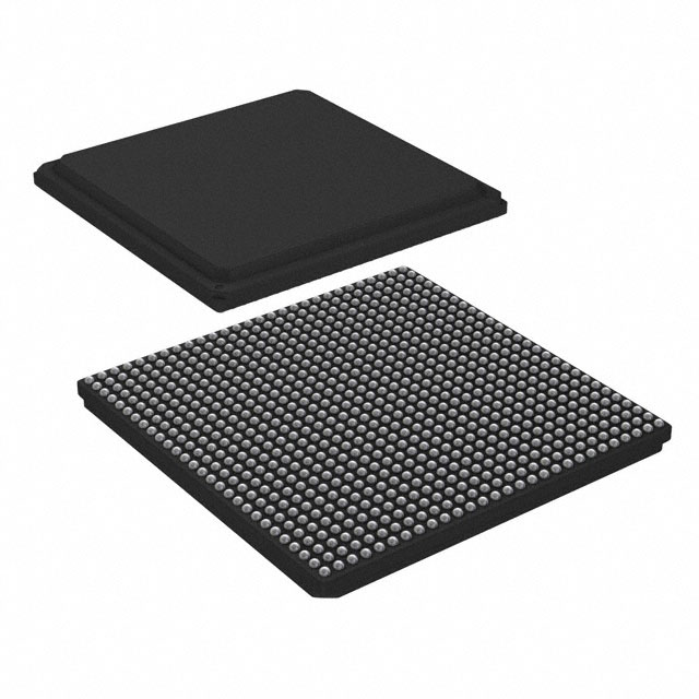
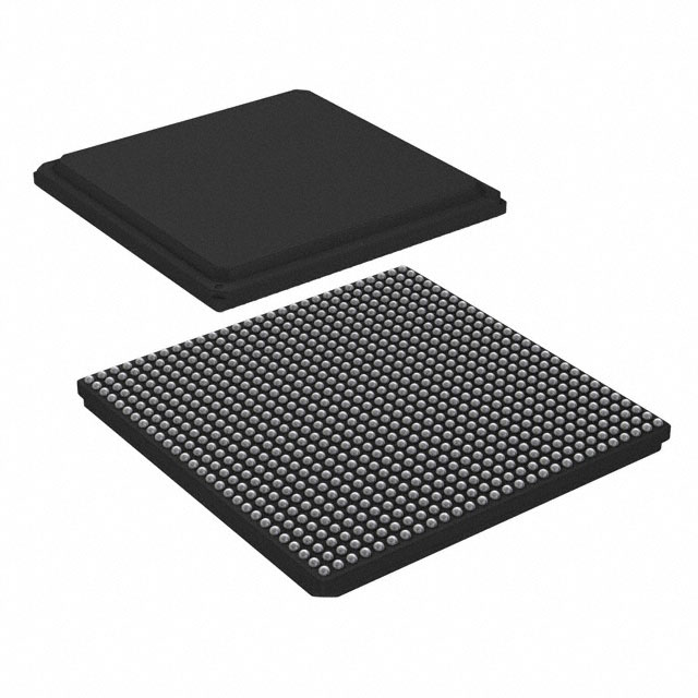
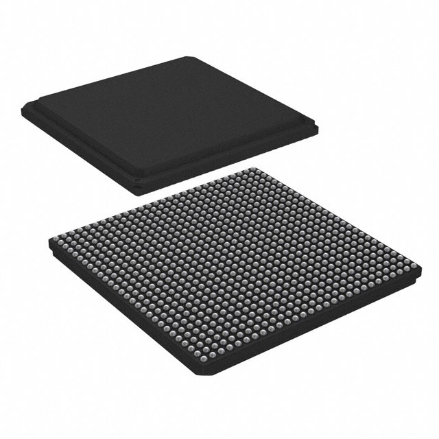
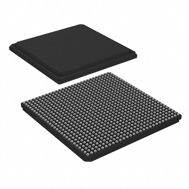
ARM® Cortex®-A72 Microprocessor IC QorIQ® Layerscape 4 Core, 64-Bit 1.6GHz 780-FCPBGA (23x23) |
|---|---|
| Quantity | 195 Available (as of October 8, 2026) |
| Product Category | Microprocessors |
|---|---|
| Part Series | LS1046A |
| Manufacturer | NXP USA Inc. |
| Manufacturing Status | Active |
| Manufacturer Standard Lead Time | 18 Weeks |
| Datasheet |
Specifications & Environmental
| Core Processor | ARM® Cortex®-A72 | Device Package | 780-FCPBGA (23x23) | ECCN | 5A002A1 NXP | ||
|---|---|---|---|---|---|---|---|
| Ethernet | 10GbE (2), 2.5GbE (1), 1GbE (4) | HTS Code | 8542.31.0001 | Moisture Sensitivity Level | 3 (168 Hours) | ||
| Mounting Method | Surface Mount | Mounting Type | Surface Mount | Number of Cores/Bus Width | 4 Core, 64-Bit | ||
| Operating Temperature | -40°C ~ 105°C | Package / Case | 780-FBGA, FCBGA | RAM Controllers | DDR4 | ||
| REACH Compliance | REACH Unaffected | RoHS Compliance | ROHS3 Compliant | SATA | SATA 6Gbps (1) | ||
| Security Features | Secure Boot, TrustZone® | Speed | 1.6GHz | Supplier Device Package | 780-FCPBGA (23×23) | ||
| USB | USB 3.0 (3) + PHY |
Overview of LS1046AXE8Q1A – IC MPU QORIQ 1.6GHZ 780FCPBGA
The LS1046AXE8Q1A is an NXP QorIQ Layerscape microprocessor featuring four ARM® Cortex®‑A72 64‑bit cores running at 1.6 GHz in a single cluster. It integrates high‑performance packet and data‑path acceleration together with broad peripheral support to address embedded and industrial applications that require multi‑core processing, secure operation, and rich I/O.
Built for industrial environments, the device combines DDR4 memory support with multiple high‑speed networking interfaces, storage and USB connectivity, and hardware security features—delivering a compact, industrially qualified MPU in a 780‑FCPBGA 23 mm × 23 mm package.
Key Features
- CPU Core — Four ARM® Cortex®‑A72 64‑bit cores arranged as a single cluster with a shared L2 cache; single‑threaded cores optimized for embedded multi‑core workloads at 1.6 GHz.
- Memory Subsystem — Integrated DDR4 SDRAM controller with ECC and interleaving support for reliable system memory operation.
- High‑Speed Networking — Multiple Ethernet options including 2 × 10GbE, 1 × 2.5GbE and 4 × 1GbE interfaces to support diverse networking topologies and throughput requirements.
- Data Path Acceleration (DPAA) — On‑chip acceleration for packet parsing/classification (FMan), queue and buffer management (QMan/BMan), cryptography acceleration (SEC), and IEEE 1588 support to offload networking tasks from the CPU.
- Peripheral and Storage Interfaces — SATA 6Gbps controller, three USB 3.0 controllers with integrated PHY, three PCIe 3.0 controllers, QSPI/SPI and integrated flash controller supporting NAND/NOR; expanded device connectivity for embedded systems.
- Security — Secure Boot and TrustZone® support plus on‑chip cryptography acceleration for protected boot and runtime security functions.
- Package and Reliability — 780‑FBGA (780‑FCPBGA) 23 mm × 23 mm surface‑mount package; industrial qualification with operating temperature range of −40 °C to 105 °C.
Typical Applications
- Industrial Networking and Control — Leverages multiple Ethernet ports and DPAA packet acceleration to implement real‑time networked control and industrial communication stacks.
- Edge and Gateway Devices — Combines multi‑core compute, DDR4 memory with ECC, and secure boot features to host edge applications that require local processing and secure connectivity.
- Storage and NAS Appliances — Integrated SATA 6Gbps, eMMC/SD host support and NAND/NOR flash controller enable compact storage controllers and networked storage solutions.
- Secure Connectivity Platforms — Hardware cryptography acceleration plus TrustZone® and Secure Boot support secure data plane and device authentication implementations.
Unique Advantages
- High aggregate I/O bandwidth: Multiple 10GbE/2.5GbE/1GbE ports, SATA 6Gbps, PCIe 3.0 and USB 3.0 provide broad high‑speed connectivity without external bridges.
- Offloaded packet processing: DPAA components (FMan/QMan/BMan) reduce CPU load for packet parsing, scheduling and buffer management, simplifying network stack design.
- Integrated security toolkit: Secure Boot, TrustZone® and cryptography acceleration enable secure system designs with reduced software overhead.
- Industrial temperature capability: −40 °C to 105 °C operating range and industrial qualification support deployment in temperature‑challenging environments.
- Compact, production‑ready package: 780‑FCPBGA (23 × 23 mm) surface‑mount package provides a high‑density, manufacturable footprint for embedded PCBs.
- Rich peripheral set: On‑chip DDR4 controller with ECC, multiple USB/PCIe controllers, SATA and integrated flash interfaces lower BOM and simplify board design.
Why Choose LS1046AXE8Q1A?
The LS1046AXE8Q1A positions itself as a balanced, highly integrated MPU for embedded and industrial designs that require multi‑core compute, robust networking and built‑in security. Its combination of ARM® Cortex®‑A72 cores, DDR4 with ECC, extensive high‑speed I/O and DPAA acceleration makes it suitable for gateway, edge compute, secure communications and storage controller applications.
Designed and supplied by NXP Semiconductors, the LS1046A family provides a pathway for scalable deployments where performance, integration, and industrial reliability are important. The device’s integrated peripherals and hardware acceleration reduce external components and simplify system architecture for long‑term, maintainable designs.
Request a quote or submit an inquiry to receive pricing, availability, and technical support for the LS1046AXE8Q1A. Our team can assist with lead times, volume pricing and integration considerations to help accelerate your design.



















Date Founded: 2006
Headquarters: Eindhoven, North Brabant, Netherlands
Employees: 38,000+
Revenue: $10.53 Billion
Certifications and Memberships: ISO9001:2015, IATF16949:2016


