
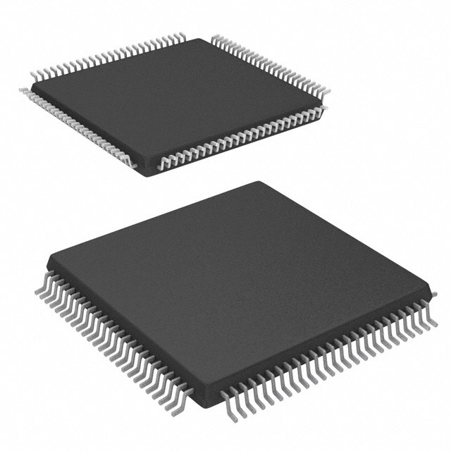
A3PN060-Z1VQ100
| Part Description |
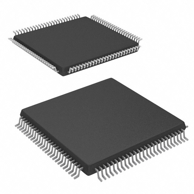
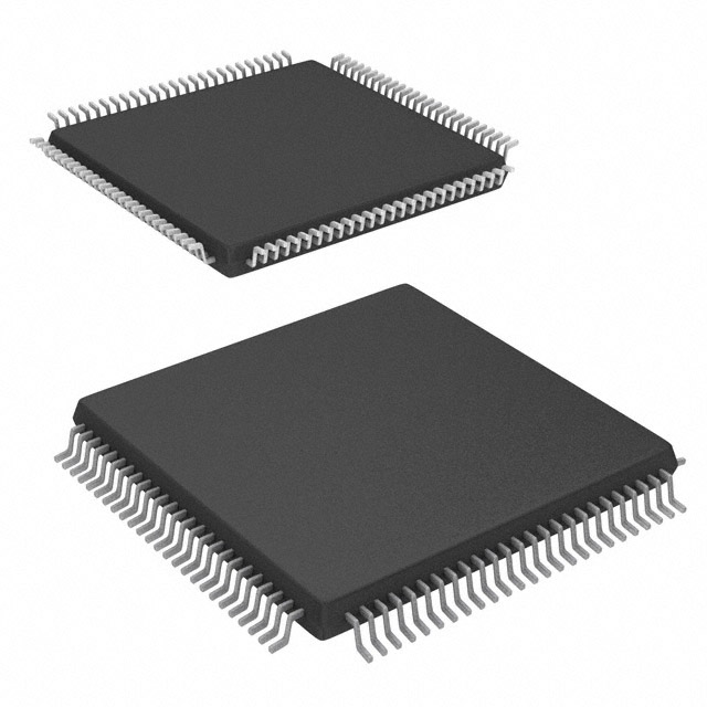
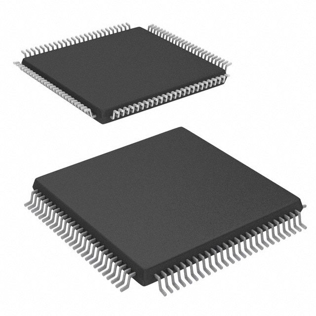
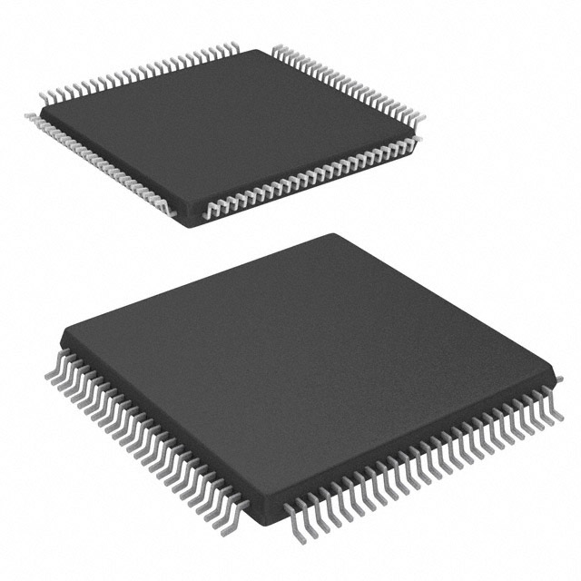
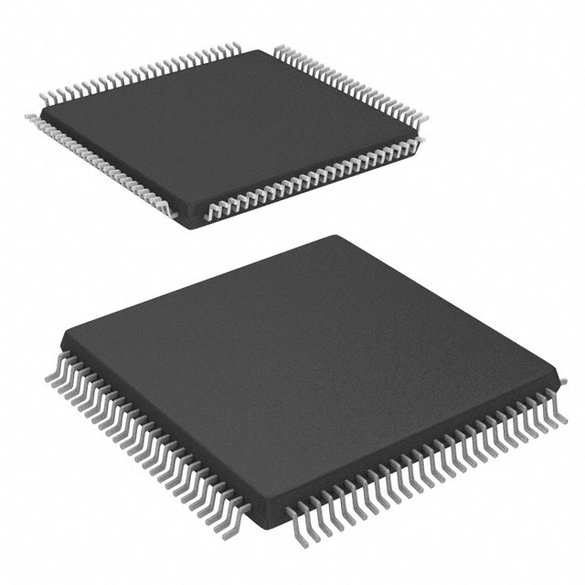
ProASIC3 nano Field Programmable Gate Array (FPGA) IC 71 18432 100-TQFP |
|---|---|
| Quantity | 622 Available (as of October 7, 2026) |
| Product Category | Field Programmable Gate Array (FPGA) |
|---|---|
| Manufacturer | Microchip Technology |
| Manufacturing Status | Obsolete |
| Manufacturer Standard Lead Time | Contact Us |
| Datasheet |
Specifications & Environmental
| Device Package | 100-VQFP (14x14) | Grade | Commercial | Operating Temperature | -20°C – 85°C | ||
|---|---|---|---|---|---|---|---|
| Package / Case | 100-TQFP | Number of I/O | 71 | Voltage | 1.425 V - 1.575 V | ||
| Mounting Method | Surface Mount | RoHS Compliance | RoHS non-compliant | REACH Compliance | REACH Unaffected | ||
| Moisture Sensitivity Level | 3 (168 Hours) | Number of LABs/CLBs | 1536 | Number of Logic Elements/Cells | 1536 | ||
| Number of Gates | 60000 | ECCN | 3A991D | HTS Code | 8542.39.0001 | ||
| Qualification | N/A | Total RAM Bits | 18432 |
Overview of A3PN060-Z1VQ100 – ProASIC3 nano Field Programmable Gate Array (FPGA) IC, 71 I/Os, 100‑TQFP
The A3PN060-Z1VQ100 from Microchip Technology is a ProASIC3 nano flash-based FPGA offered in a 100‑TQFP (14×14 mm) package. The device integrates 1,536 logic elements (cells) and approximately 60,000 gates with 18,432 bits of on‑chip RAM, delivering a compact, low‑power FPGA fabric for space-constrained, commercial-grade embedded designs.
Built for low-power flash devices, the ProASIC3 nano architecture includes support for multiple low-power modes and global resource structures described in the device documentation, making it suitable for applications that require flexible logic, moderate embedded memory, and a fixed 71 I/O pin count.
Key Features
- Logic Resources — 1,536 logic elements (cells) providing approximately 60,000 gates for custom digital logic and glue‑logic integration.
- Embedded Memory — 18,432 bits of on‑chip RAM for small FIFOs, registers, and buffering needs within the FPGA fabric.
- I/O Density — 71 general-purpose I/Os available in the 100‑TQFP package for sensor, control, and peripheral interfaces.
- Low-Power Flash FPGA Fabric — Device documentation details low-power modes (Static/Idle, Sleep, Shutdown) and a fabric optimized for flash-based configurations.
- Global Resources & Clocking — Architecture documentation shows support for global resources and clock aggregation to manage clock distribution across the array.
- Power Supply — Narrow core voltage range of 1.425 V to 1.575 V for predictable supply requirements.
- Package & Mounting — 100‑TQFP (supplier package: 100‑VQFP, 14×14 mm) surface-mount package for standard PCB assembly.
- Operating Range — Commercial-grade operating temperature from -20 °C to 85 °C and RoHS compliance for regulatory handling.
Typical Applications
- Embedded Control Logic — Use the 1,536 logic elements to implement finite-state machines, protocol bridges, and application-specific control functions.
- Sensor and I/O Aggregation — 71 I/Os provide the pin count needed for aggregating sensors, switches, and simple actuator interfaces on compact boards.
- Glue Logic and Peripheral Interfaces — Small amounts of on‑chip RAM and moderate gate density make the device suitable for custom interfacing and timing adaptation between system blocks.
Unique Advantages
- Compact FPGA Fabric: 1,536 logic elements and 18,432 bits of RAM deliver useful programmable capacity in a small 100‑TQFP footprint, reducing board area for compact designs.
- Flash-Based Low-Power Architecture: The ProASIC3 nano family documentation highlights multiple low-power modes, enabling reduced standby consumption where applicable.
- Predictable Power Supply Window: A defined core supply range (1.425–1.575 V) simplifies power rail design and component selection.
- Commercial Temperature Range: Rated for -20 °C to 85 °C to match typical commercial embedded product requirements.
- Standard Surface-Mount Package: The 100‑TQFP surface-mount package supports conventional PCB assembly and prototyping workflows.
- Regulatory Compliance: RoHS compliance reduces material-related constraints for commercial product builds.
Why Choose A3PN060-Z1VQ100?
The A3PN060-Z1VQ100 positions itself as a compact, low‑power flash FPGA option for commercial embedded designs that need moderate logic density, a controlled on‑chip RAM footprint, and a fixed set of I/Os in a standard 100‑TQFP package. Its documented low-power modes and global resource architecture provide design flexibility for projects where power management and predictable clock/resource distribution matter.
This device is well suited to design teams looking for a small-footprint, flash-configured FPGA from Microchip Technology to implement glue logic, I/O aggregation, and control functions while keeping BOM complexity and board area to a minimum.
Request a quote or submit a request for pricing and availability to move your design forward with the A3PN060-Z1VQ100.





















Date Founded: 1989
Headquarters: Chandler, Arizona, USA
Employees: 22,000+
Revenue: $8.349 Billion
Certifications and Memberships: ISO9001:2015, IATF16949:2016, AS 9100D




