
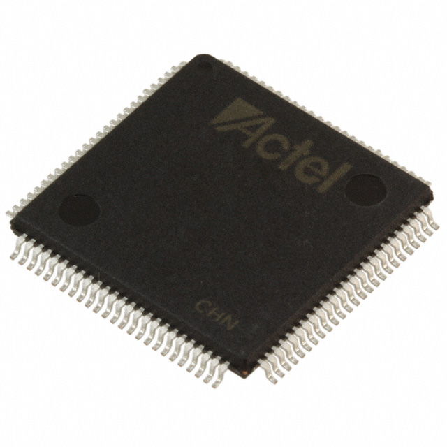
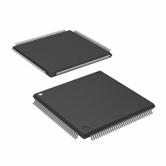
A54SX08A-1TQG144I
| Part Description |
SX-A Field Programmable Gate Array (FPGA) IC 113 144-LQFP |
|---|---|
| Quantity | 634 Available (as of June 15, 2026) |

| Product Category | Field Programmable Gate Array (FPGA) |
|---|---|
| Manufacturer | Microchip Technology |
| Manufacturing Status | Active |
| Manufacturer Standard Lead Time | 12 Weeks |
| Datasheet |
Specifications & Environmental
| Device Package | 144-TQFP (20x20) | Grade | Industrial | Operating Temperature | -40°C – 85°C | ||
|---|---|---|---|---|---|---|---|
| Package / Case | 144-LQFP | Number of I/O | 113 | Voltage | 2.25 V - 5.25 V | ||
| Mounting Method | Surface Mount | RoHS Compliance | ROHS3 Compliant | REACH Compliance | REACH Unaffected | ||
| Moisture Sensitivity Level | 3 (168 Hours) | Number of LABs/CLBs | 768 | Number of Logic Elements/Cells | 768 | ||
| Number of Gates | 12000 | ECCN | 3A991D | HTS Code | 8542.39.0001 | ||
| Qualification | N/A |
Overview of A54SX08A-1TQG144I – SX-A Field Programmable Gate Array (FPGA), 113 I/Os, 144-LQFP
The A54SX08A-1TQG144I is an SX-A family FPGA in a 144-pin LQFP/TQFP package, offering 12,000 system gates and 768 logic elements for mid-density programmable logic tasks. Designed for industrial-temperature operation, this nonvolatile single-chip FPGA provides mixed-voltage I/O support and a compact surface-mount package suitable for embedded control, interface bridging, and moderate-complexity digital processing.
Key Features
- Core Performance — System performance up to 250 MHz and internal performance up to 350 MHz as specified for the SX-A family; part includes the –1 speed grade for increased speed relative to standard devices.
- Logic Density — 12,000 system gates and 768 logic elements provide a mid-range programmable fabric for combinatorial and sequential logic implementation.
- Flip-Flops / Registers — Device-level resources include dedicated flip-flops (family data shows up to 2,012 flip-flops across devices in the family).
- I/O and Voltage Flexibility — 113 user I/Os in the 144-pin package with configurable I/O support for 3.3 V / 5 V PCI, 5 V TTL, 3.3 V LVTTL and 2.5 V LVCMOS2 standards; devices support mixed 2.5 V, 3.3 V, and 5 V operation with 5 V input tolerance and 5 V drive strength.
- Power and Reliability — Hot-swap compliant I/Os, power-up/power-down friendly operation (no sequencing required), configurable weak pull-up/pull-down on I/O at power-up, and individual output slew-rate control.
- Configuration and Security — Nonvolatile single-chip solution with Actel Secure Programming Technology (FuseLock™) to protect design IP and prevent reverse engineering.
- System Test and Debug — Boundary-scan testing compliant with IEEE 1149.1 (JTAG) and unique in-system diagnostic/verification capability available with Silicon Explorer II.
- Package and Mounting — Surface-mount 144-LQFP package (supplier device package listed as 144-TQFP, 20×20); RoHS-compliant packaging.
- Industrial Temperature Grade — Rated for operation from –40 °C to 85 °C.
Typical Applications
- Industrial Control — Implement motor control logic, timing, and custom digital interfaces that benefit from industrial-temperature operation and flexible I/O standards.
- Interface Bridging — Use the FPGA to bridge mixed-voltage peripherals and manage protocol translation where multiple I/O standards and 5 V tolerance are required.
- Embedded System Glue Logic — Replace discrete glue components with a single programmable device to consolidate control, bus arbitration, and peripheral timing functions.
- In-System Test and Verification — Integrate boundary-scan and Silicon Explorer II diagnostics for manufacturing test and field verification workflows.
Unique Advantages
- Compact, Nonvolatile Integration: A single-chip, nonvolatile FPGA reduces external configuration components and simplifies system power sequencing.
- Flexible Mixed-Voltage I/O: Native support for 2.5 V, 3.3 V, and 5 V signaling with 5 V input tolerance enables straightforward interfacing with a wide range of legacy and modern peripherals.
- Industrial Reliability: Rated for –40 °C to 85 °C operation and available in a surface-mount 144-pin package suitable for production embedded designs.
- IP Protection: Built-in FuseLock technology helps protect design intellectual property against reverse engineering.
- Built-In Testability: IEEE 1149.1 boundary-scan and in-system diagnostics support streamlined manufacturing test and field troubleshooting.
- Deterministic Timing Control: SX-A family features deterministic, user-controllable timing useful for designs that require predictable timing closure.
Why Choose A54SX08A-1TQG144I?
The A54SX08A-1TQG144I targets designs that need a mid-density, nonvolatile FPGA with flexible I/O voltage support and industrial-temperature capability. With 12,000 system gates and 768 logic elements, it consolidates glue logic, interface translation, and moderate-complexity state machines into a single surface-mount device while providing built-in security and test support.
For teams balancing integration, configurability, and reliability, this SX-A family part offers a practical platform that aligns with industrial embedded applications and production test flows, backed by family-level features such as deterministic timing, hot-swap I/O behavior, and in-system diagnostic capabilities.
Request a quote or contact sales to check availability and pricing for the A54SX08A-1TQG144I and to discuss volume, lead time, or technical integration support.


Date Founded: 1989
Headquarters: Chandler, Arizona, USA
Employees: 22,000+
Revenue: $8.349 Billion
Certifications and Memberships: ISO9001:2015, IATF16949:2016, AS 9100D


