
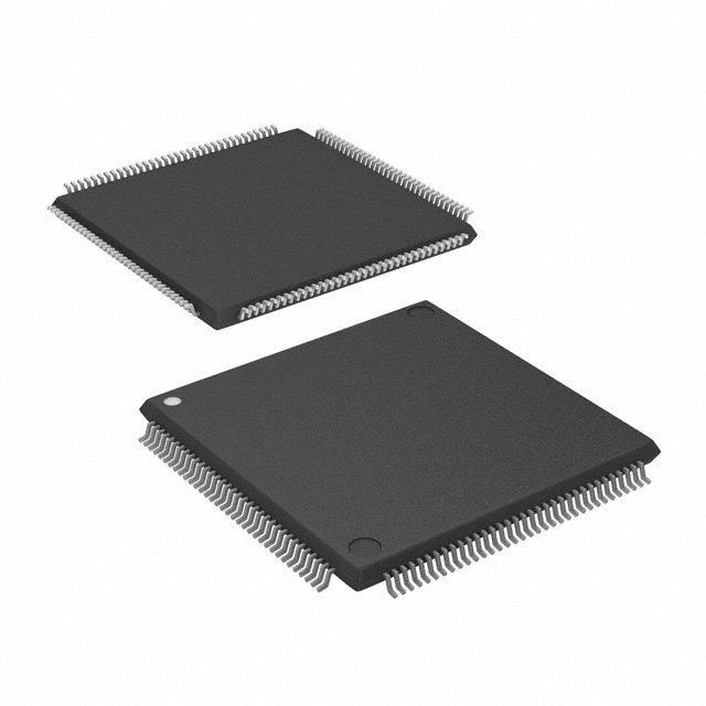
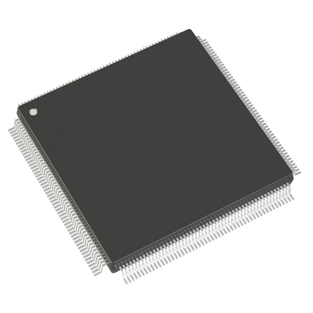
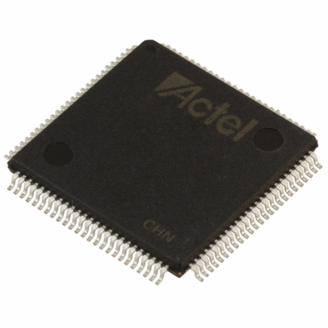
A54SX16A-FPQ208
| Part Description |
SX-A Field Programmable Gate Array (FPGA) IC 175 208-BFQFP |
|---|---|
| Quantity | 1,360 Available (as of June 14, 2026) |

| Product Category | Field Programmable Gate Array (FPGA) |
|---|---|
| Manufacturer | Microchip Technology |
| Manufacturing Status | Obsolete |
| Manufacturer Standard Lead Time | Contact Us |
| Datasheet |
Specifications & Environmental
| Device Package | 208-PQFP (28x28) | Grade | Commercial | Operating Temperature | 0°C – 70°C | ||
|---|---|---|---|---|---|---|---|
| Package / Case | 208-BFQFP | Number of I/O | 175 | Voltage | 2.25 V - 5.25 V | ||
| Mounting Method | Surface Mount | RoHS Compliance | RoHS non-compliant | REACH Compliance | REACH Unaffected | ||
| Moisture Sensitivity Level | 3 (168 Hours) | Number of LABs/CLBs | 1452 | Number of Logic Elements/Cells | 1452 | ||
| Number of Gates | 24000 | ECCN | 3A991D | HTS Code | 8542.39.0001 | ||
| Qualification | N/A |
Overview of A54SX16A-FPQ208 – SX-A Field Programmable Gate Array (FPGA) IC 175 208-BFQFP
The A54SX16A-FPQ208 is a member of the SX-A family of nonvolatile FPGAs from Microchip Technology. It delivers 24,000 system gates with 1,452 logic elements and up to 175 user-programmable I/O pins in a 208-pin surface-mount package.
Designed for mixed-voltage, single-chip implementations, this commercial-grade FPGA is suited to designs requiring configurable I/O, deterministic timing and hardware-level security features for IP protection and in-system verification.
Key Features
- Capacity & Logic — 24,000 system gates and 1,452 logic elements provide mid-range programmable logic density for interface and control functions.
- I/O Count & Flexibility — Up to 175 user-programmable I/O pins with configurable I/O support for 3.3 V / 5 V PCI, 5 V TTL, 3.3 V LVTTL and 2.5 V LVCMOS2 signaling.
- Mixed‑Voltage Operation — Supports 2.5 V, 3.3 V and 5 V mixed-voltage operation with 5 V input tolerance and 5 V drive strength; supply range 2.25 V to 5.25 V.
- Performance — Family-level documented performance includes up to 350 MHz internal performance and up to 250 MHz system performance.
- Packaging & Mounting — 208-pin BFQFP package; supplier device package listed as 208-PQFP (28×28). Surface-mount mounting type.
- Power & Board Friendliness — Power-up/down friendly (no sequencing required for supply voltages) and hot-swap compliant I/Os to simplify system integration.
- Programmability & Security — Nonvolatile single-chip configuration and Actel Secure Programming Technology (FuseLock) for protecting designs against reverse engineering.
- Test & Diagnostics — In-system diagnostic and verification support with Silicon Explorer II and boundary-scan testing compliant with IEEE 1149.1 (JTAG).
- Operating Range & Compliance — Commercial temperature grade (0 °C to 70 °C) and RoHS compliant.
Typical Applications
- PCI Interface Logic — Use the device’s 66 MHz PCI compliance and configurable I/O to implement PCI interface glue logic and bridging functions.
- Mixed‑Voltage I/O Bridging — Mixed-voltage operation and 5 V tolerant I/Os enable level translation and interface control across 2.5 V, 3.3 V and 5 V domains.
- Hot‑Swap Systems — Hot-swap compliant I/Os and power-up/down friendly behavior make the FPGA suitable for replaceable or live-insert modules requiring safe board insertion/removal.
- In‑System Diagnostic & Verification — Built-in in-system diagnostic capability supports runtime validation and debugging using Silicon Explorer II and JTAG boundary-scan.
Unique Advantages
- Nonvolatile Single‑Chip Solution: Eliminates the need for external configuration memory and simplifies board-level BOM and system initialization.
- Flexible Mixed‑Voltage I/O: Reduces external level-shifting components by supporting multiple I/O standards and 5 V tolerance on inputs.
- Deterministic Timing Control: Family-level deterministic, user-controllable timing helps streamline timing closure for predictable system behavior.
- Integrated Security Features: FuseLock secure programming protects intellectual property and prevents reverse engineering of deployed designs.
- Board-Level Friendliness: Hot-swap I/Os and no required supply sequencing reduce integration complexity for modular or serviceable systems.
- Standards-Based Testability: IEEE 1149.1 boundary-scan support enables structured manufacturing test and in-field diagnostics.
Why Choose A54SX16A-FPQ208?
The A54SX16A-FPQ208 positions itself as a compact, nonvolatile FPGA for mid-density logic requirements where mixed-voltage interfacing, in-system diagnostics and IP protection are priorities. With 24,000 system gates, 1,452 logic elements and up to 175 I/Os in a 208-pin surface-mount package, it fits designs that need a reliable single-chip programmable solution without external configuration memory.
This device is ideal for engineers building mixed-voltage interfaces, PCI-related logic, hot-swap-capable modules and systems that benefit from built-in diagnostics and boundary-scan testability. Its RoHS-compliant, commercial-grade specification and family-level development tools support predictable integration and lifecycle support.
Request a quote or submit an inquiry to get pricing and availability for the A54SX16A-FPQ208 and to discuss how it fits your next design.


Date Founded: 1989
Headquarters: Chandler, Arizona, USA
Employees: 22,000+
Revenue: $8.349 Billion
Certifications and Memberships: ISO9001:2015, IATF16949:2016, AS 9100D


