
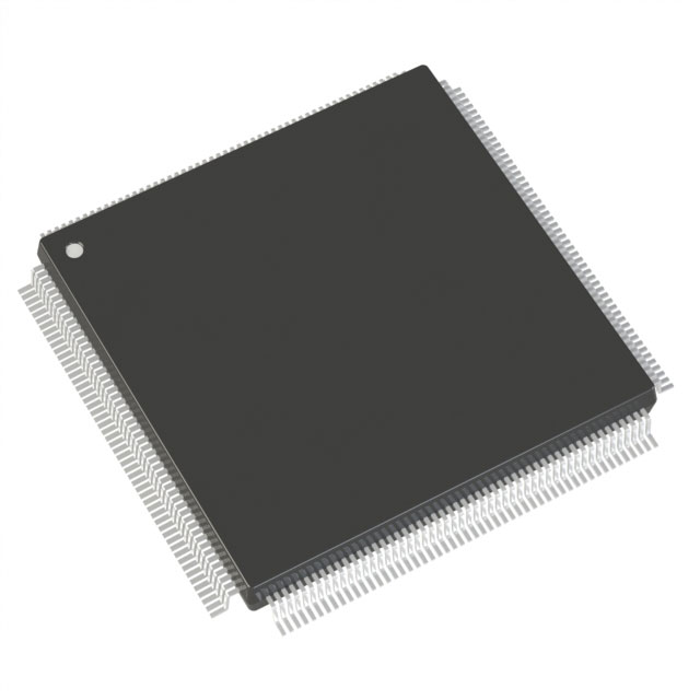
A54SX72A-PQG208
| Part Description |
SX-A Field Programmable Gate Array (FPGA) IC 171 208-BFQFP |
|---|---|
| Quantity | 487 Available (as of June 15, 2026) |

| Product Category | Field Programmable Gate Array (FPGA) |
|---|---|
| Manufacturer | Microchip Technology |
| Manufacturing Status | Active |
| Manufacturer Standard Lead Time | 14 Weeks |
| Datasheet |
Specifications & Environmental
| Device Package | 208-PQFP (28x28) | Grade | Commercial | Operating Temperature | 0°C – 70°C | ||
|---|---|---|---|---|---|---|---|
| Package / Case | 208-BFQFP | Number of I/O | 171 | Voltage | 2.25 V - 5.25 V | ||
| Mounting Method | Surface Mount | RoHS Compliance | ROHS3 Compliant | REACH Compliance | REACH Unaffected | ||
| Moisture Sensitivity Level | 3 (168 Hours) | Number of LABs/CLBs | 6036 | Number of Logic Elements/Cells | 6036 | ||
| Number of Gates | 108000 | ECCN | 3A991D | HTS Code | 8542.39.0001 | ||
| Qualification | N/A |
Overview of A54SX72A-PQG208 – SX-A Field Programmable Gate Array (FPGA) IC 171 208-BFQFP
The A54SX72A-PQG208 is a nonvolatile SX-A family FPGA from Microchip Technology in a 208-pin PQFP surface-mount package. It provides 108,000 system gates implemented as approximately 6,036 logic elements and up to 171 user I/Os, delivering a compact, reprogrammable logic solution for commercial embedded designs.
Designed for mixed-voltage systems, the device supports a 2.25 V to 5.25 V supply range, hot-swap–compliant I/Os and PCI‑capable interfaces. Key value propositions include single-chip nonvolatile operation, configurable I/O flexibility, deterministic timing control and on-board security features referenced in the SX-A family datasheet.
Key Features
- Logic Capacity 108,000 system gates implemented as approximately 6,036 logic elements and up to 2,012 dedicated flip-flops (up to 4,024 maximum flip-flops with cell configurations).
- I/O and Clocking Up to 171 user-programmable I/O pins in the 208-pin PQFP package, with three global clocks and four quadrant clocks for flexible clock distribution.
- Performance System performance up to 250 MHz and internal performance up to 350 MHz as specified for the SX-A family.
- Voltage and I/O Flexibility Supports mixed-voltage operation from 2.5 V, 3.3 V and 5 V ranges with 5 V input tolerance and selectable I/O standards and drive strength; overall supply range 2.25 V to 5.25 V.
- Nonvolatile Single-Chip Solution On-chip nonvolatile configuration removes the need for an external configuration memory device.
- System and Power-Friendly I/Os Hot-swap–compliant I/Os and power-up/power-down friendly operation that does not require sequencing of supply voltages.
- Security and Test Family features include Actel Secure Programming Technology (FuseLock™) to protect bitstream IP and IEEE 1149.1 (JTAG) boundary-scan support for board-level testability.
- Package and Compliance 208-pin plastic quad flat pack (PQFP) surface-mount package; RoHS compliant and specified for commercial temperature operation (0 °C to +70 °C).
- Memory No on-chip embedded RAM (Total RAM bits: 0), delivering a logic-focused resource profile for glue logic and I/O-centric applications.
Typical Applications
- Mixed-Voltage Interface Control Reconfigurable I/O support for 5 V, 3.3 V and 2.5 V interfaces makes the device suitable for bridging and level-shifting tasks in commercial systems.
- PCI-Capable Logic With 66 MHz PCI compliance noted for the SX-A family, the device can be used for PCI-related glue logic and interface functions.
- Embedded System Glue Logic Compact, nonvolatile FPGA for replacing multiple discrete components in commercial embedded designs requiring reprogrammable logic.
- Secure, In-System Programmable Designs Use the device where in-field reconfiguration with bitstream protection and JTAG testability are required.
Unique Advantages
- Nonvolatile, single-chip configuration: Eliminates external configuration memory and simplifies BOM and board-level design.
- Flexible mixed-voltage I/Os: Configurable I/O standards and 5 V input tolerance allow direct interfacing to a wide range of commercial logic levels.
- High logic density in PQFP package: 108,000 system gates and ~6,036 logic elements in a 208-pin package provide significant integration for compact designs.
- Deterministic timing and clock resources: Dedicated global and quadrant clocks enable predictable timing architectures for synchronous designs.
- Security and testability: FuseLock™ programming protection and IEEE 1149.1 boundary-scan support improve IP protection and production test coverage.
- Commercial temperature and RoHS compliance: Designed for commercial-grade deployments (0 °C to +70 °C) and RoHS-compliant materials and packaging.
Why Choose A54SX72A-PQG208?
The A54SX72A-PQG208 combines a high logic gate count and configurable I/O flexibility in a single nonvolatile FPGA package suited for commercial embedded applications. Its mix of performance (up to 250 MHz system, 350 MHz internal), deterministic clocking resources and on-chip security features supports designs that require reprogrammable logic, secure bitstream handling and robust board-level testability.
This device is well suited to engineers and designers who need a reprogrammable, nonvolatile logic device for mixed-voltage interfaces, PCI-capable glue logic and compact embedded systems where surface-mount PQFP packaging and commercial temperature operation meet project requirements.
Request a quote or submit an inquiry to receive pricing and availability for the A54SX72A-PQG208 and support for your integration and procurement needs.


Date Founded: 1989
Headquarters: Chandler, Arizona, USA
Employees: 22,000+
Revenue: $8.349 Billion
Certifications and Memberships: ISO9001:2015, IATF16949:2016, AS 9100D


