
AGLN125V2-ZCSG81
| Part Description |
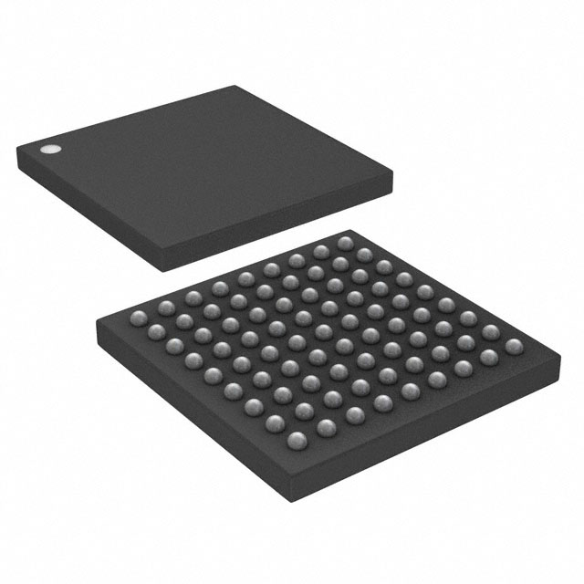
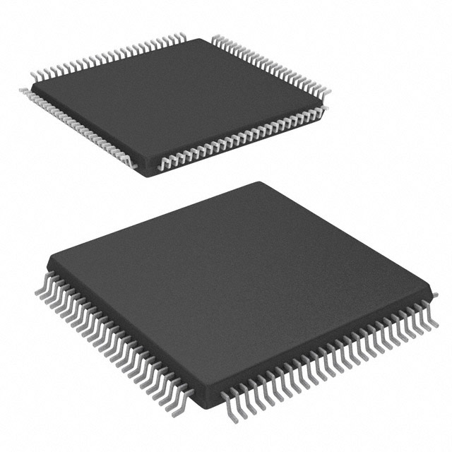
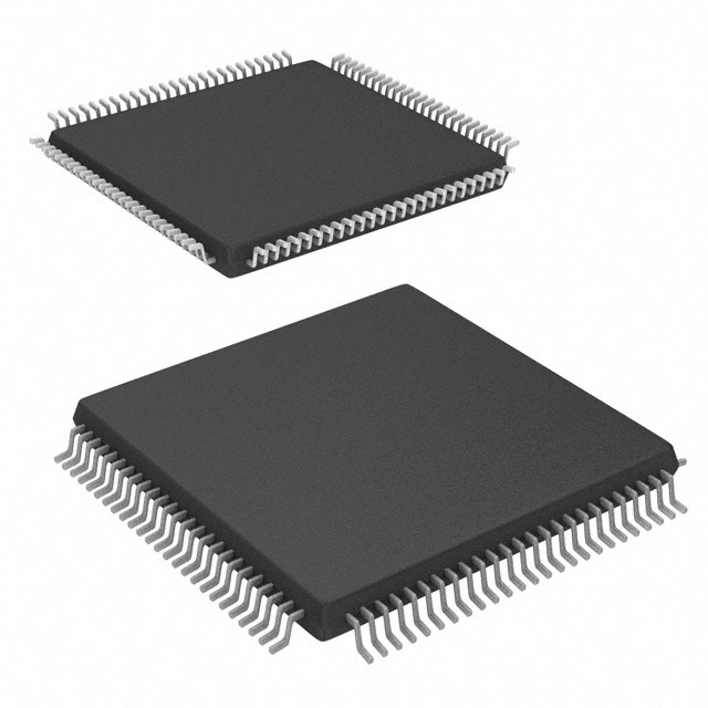
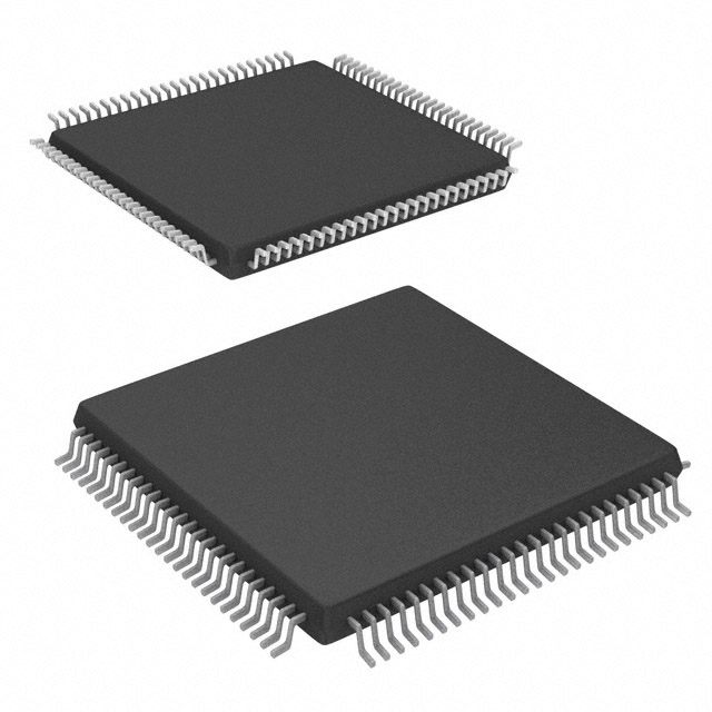
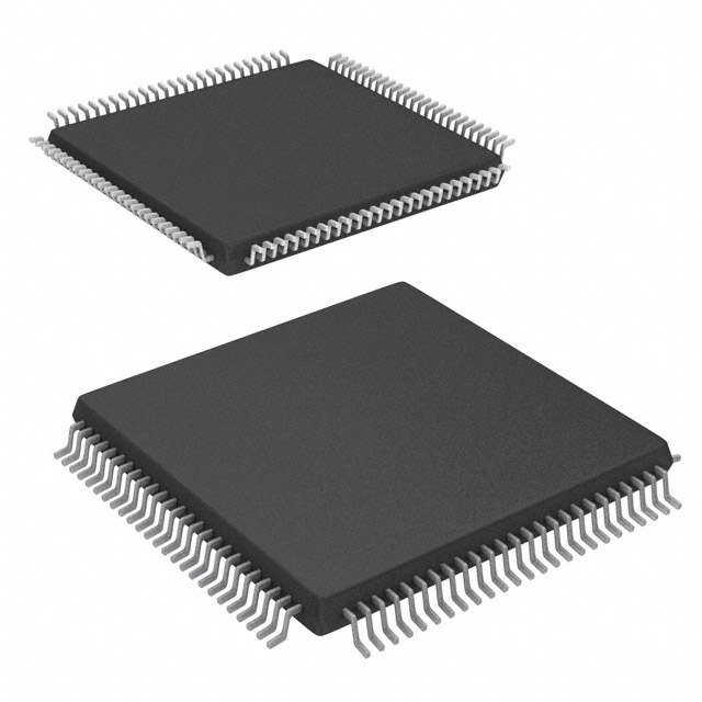
IGLOO nano Field Programmable Gate Array (FPGA) IC 60 36864 3072 81-WFBGA, CSBGA |
|---|---|
| Quantity | 1,074 Available (as of October 8, 2026) |
| Product Category | Field Programmable Gate Array (FPGA) |
|---|---|
| Manufacturer | Microchip Technology |
| Manufacturing Status | Obsolete |
| Manufacturer Standard Lead Time | Contact Us |
| Datasheet |
Specifications & Environmental
| Device Package | 81-CSP (5x5) | Grade | Commercial | Operating Temperature | -20°C – 85°C | ||
|---|---|---|---|---|---|---|---|
| Package / Case | 81-WFBGA, CSBGA | Number of I/O | 60 | Voltage | 1.14 V - 1.575 V | ||
| Mounting Method | Surface Mount | RoHS Compliance | Unknown | REACH Compliance | REACH Unaffected | ||
| Moisture Sensitivity Level | 3 (168 Hours) | Number of LABs/CLBs | 3072 | Number of Logic Elements/Cells | 3072 | ||
| Number of Gates | 125000 | ECCN | 3A991D | HTS Code | 8542.39.0001 | ||
| Qualification | N/A | Total RAM Bits | 36864 |
Overview of AGLN125V2-ZCSG81 – IGLOO nano FPGA, 3072 logic elements, 36,864 bits RAM, 60 I/Os
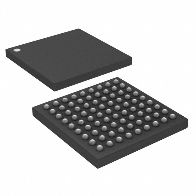
The AGLN125V2-ZCSG81 is a Microchip Technology IGLOO nano family Field Programmable Gate Array (FPGA) supplied in an 81-pin WFBGA/CSBGA package. It combines reprogrammable flash-based configuration with low-voltage operation to address space-constrained, low-power embedded designs.
With 3,072 logic elements, 36,864 bits of on-chip RAM and 60 user I/Os, this device targets applications that require compact footprint, nonvolatile configuration retention and reduced standby power through Flash*Freeze technology.
Key Features
- Core Logic – 3,072 logic elements (versatile fabric equivalent) and approximately 125,000 system gates provide the configurable logic resources for custom digital functions.
- Embedded Memory – 36,864 bits of on-chip SRAM organized in variable-aspect 4,608-bit RAM blocks; includes 1 kbit of FlashROM user nonvolatile memory for on-chip storage.
- I/O Flexibility – 60 user I/Os with series-level support for mixed-voltage operation (1.2 V, 1.5 V, 1.8 V, 2.5 V and 3.3 V) and bank-selectable I/O voltages (up to 4 banks per chip).
- Low-Voltage Supply – Core supply rating from 1.14 V to 1.575 V to match low-voltage system rails.
- Low-Power Operation – Flash*Freeze technology and nanoPower design enable ultra-low power retention while maintaining FPGA content when powered down.
- Reprogrammable Flash Configuration – Flash-based CMOS process provides instant-on support and retains programmed design when powered off; supports in-system programming (ISP) and secure programming features.
- Security & ISP – Series-level support for on-chip 128-bit AES decryption for ISP and FlashLock security features to protect FPGA contents.
- Performance – Series references up to 250 MHz operation at 1.5 V and 160 MHz at 1.2 V system supplies for system timing targets.
- Package & Mounting – Surface-mount package in 81-WFBGA (CSBGA); supplier device package listed as 81-CSP (5×5).
- Operating Range – Commercial temperature grade with an operating range of –20 °C to +85 °C.
Typical Applications
- Battery-powered and portable devices – Low-voltage core supply and Flash*Freeze retention reduce standby and overall power consumption for handheld or battery-operated products.
- IoT and edge sensor nodes – Small package footprint, mixed-voltage I/Os and nonvolatile configuration make it suitable for compact edge processing and sensor interfacing.
- Consumer electronics and user interfaces – Instant-on behavior and flexible I/O support enable responsive control and display interfacing in consumer devices.
- Embedded control and peripheral aggregation – Sufficient logic density and on-chip SRAM support glue logic, protocol bridging and local control tasks in embedded systems.
Unique Advantages
- Nonvolatile, reprogrammable configuration: Flash-based configuration retains design when powered off and allows field reprogramming without external configuration flash.
- Ultra-low power retention: Flash*Freeze enables extremely low standby power while preserving programmed logic and state.
- Mixed-voltage I/O flexibility: Support for multiple I/O voltage domains and bank-selectable voltages simplifies interfacing to a wide range of peripherals.
- Compact, surface-mount packaging: 81-pin WFBGA/CSBGA package and 81-CSP (5×5) supplier footprint reduce PCB area for space-constrained designs.
- Secure in-system programming: On-chip 128-bit AES ISP and FlashLock protect configuration and enable secure updates.
Why Choose AGLN125V2-ZCSG81?
The AGLN125V2-ZCSG81 positions itself as a compact, low-voltage flash FPGA for designers needing nonvolatile configuration, low standby power and flexible I/O interfacing. With 3,072 logic elements, 36,864 bits of embedded SRAM and secure ISP features, it is suited to embedded applications where board space and power budget are constrained.
Its combination of reprogrammable flash, Flash*Freeze power retention and mixed-voltage I/O support offers a balance of integration and configurable performance for long-lived consumer and embedded designs that require on-board programmability and low-power operation.
If you would like pricing or availability, request a quote or submit a procurement inquiry for the AGLN125V2-ZCSG81.





















Date Founded: 1989
Headquarters: Chandler, Arizona, USA
Employees: 22,000+
Revenue: $8.349 Billion
Certifications and Memberships: ISO9001:2015, IATF16949:2016, AS 9100D




