
AT40K05-2CQC
| Part Description |
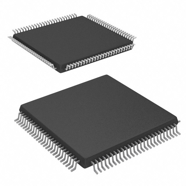
AT40K/KLV Field Programmable Gate Array (FPGA) IC 128 2048 256 160-BQFP |
|---|---|
| Quantity | 340 Available (as of June 14, 2026) |

| Product Category | Field Programmable Gate Array (FPGA) |
|---|---|
| Manufacturer | Microchip Technology |
| Manufacturing Status | Obsolete |
| Manufacturer Standard Lead Time | Contact Us |
| Datasheet |
Specifications & Environmental
| Device Package | 160-PQFP (28x28) | Grade | Commercial | Operating Temperature | 0°C – 70°C | ||
|---|---|---|---|---|---|---|---|
| Package / Case | 160-BQFP | Number of I/O | 128 | Voltage | 4.75 V - 5.25 V | ||
| Mounting Method | Surface Mount | RoHS Compliance | RoHS non-compliant | REACH Compliance | REACH Unaffected | ||
| Moisture Sensitivity Level | 3 (168 Hours) | Number of LABs/CLBs | 256 | Number of Logic Elements/Cells | 256 | ||
| Number of Gates | 10000 | ECCN | 3A991D | HTS Code | 8542.39.0001 | ||
| Qualification | N/A | Total RAM Bits | 2048 |
Overview of AT40K05-2CQC – AT40K/KLV Field Programmable Gate Array (FPGA) IC 128 2048 256 160-BQFP
The AT40K05-2CQC is an SRAM-based Field Programmable Gate Array optimized for medium-density logic designs. It delivers a combination of distributed embedded memory, reconfigurable logic, and a broad I/O complement suited for DSP coprocessor tasks, multimedia processing, and general embedded system control.
Built on the AT40K family architecture, the device offers on-chip FreeRAM memory, multi-clock support and dynamic reconfiguration capabilities while operating from a 4.75 V to 5.25 V supply and a commercial temperature range of 0 °C to 70 °C.
Key Features
- SRAM-based FPGA architecture – Configurable logic fabric with internal tri-state capability per cell for flexible signal routing and design implementations.
- Logic resources – Approximately 256 logic elements (cells) supporting roughly 10,000 usable gates for medium-complexity designs.
- Embedded memory (FreeRAM) – Approximately 2,048 bits of distributed, flexible single/dual-port 10 ns SRAM that can be used independently of logic elements for FIFOs, scratch pads and other data buffering.
- I/O density and compatibility – 128 I/Os with PCI-compliant I/O capabilities and programmable output drive; supports 3 V/5 V signaling as part of the AT40K family design options.
- Clocking – Up to eight global clocks for low-skew distribution and flexible clock domain management.
- Performance characteristics – Series-level system speeds to 100 MHz and array multipliers exceeding 50 MHz as part of the AT40K family architecture.
- Package and mounting – Delivered in a 160-BQFP package; supplier device package documented as 160-PQFP (28×28). Surface-mount mounting type.
- Power and temperature – 4.75 V to 5.25 V supply range and commercial operating temperature range of 0 °C to 70 °C.
- Compliance – RoHS compliant.
Typical Applications
- DSP coprocessor functions – Implement FIR filters, FFTs, convolvers and other arithmetic accelerators that benefit from embedded multipliers and distributed memory.
- Video and multimedia processing – Use array multipliers and on-chip memory for tasks such as compression/decompression and transform algorithms.
- High-speed I/O and protocol interfacing – 128 I/Os and PCI-compliant signaling support interface-intensive designs and system-level glue logic.
- Embedded control and prototyping – Medium-density logic and reconfigurable memory make the device suitable for rapid prototyping and control systems in commercial products.
Unique Advantages
- Integrated distributed memory – Approximately 2,048 bits of on-chip SRAM that can be allocated without consuming logic element resources, simplifying buffer and FIFO implementations.
- Dynamic reconfiguration (Cache Logic) – Family-level support for partial or full in-system reconfiguration enables adaptive designs and field updates without losing stored data.
- Multi-clock support – Eight global clocks provide flexible, low-skew clock distribution for multi-domain and high-performance designs.
- Pin and package flexibility – Offered in industry-standard 160-pin quad flat packages with pin-compatible options across the AT40K family to aid migration and board design reuse.
- Commercial-grade, RoHS compliant – Designed for commercial applications and compliant with RoHS requirements for environmental compatibility.
- Toolchain interoperability – The AT40K family integrates with industry-standard design tools for synthesis, placement and routing to accelerate development.
Why Choose AT40K05-2CQC?
The AT40K05-2CQC delivers a balance of reconfigurable logic, embedded memory and multi-clock capability in a commercial-grade, surface-mount 160-pin package. Its combination of approximately 256 logic elements, 2,048 bits of distributed SRAM and 128 I/Os makes it well suited for medium-density DSP acceleration, multimedia processing and interface-intensive embedded designs.
Designed for teams needing flexible in-system update options and established design-tool interoperability, the AT40K05-2CQC offers scalable functionality within the AT40K family for developers focusing on performance, adaptability and straightforward board-level integration.
Request a quote or submit an RFQ to get pricing and availability for the AT40K05-2CQC.


Date Founded: 1989
Headquarters: Chandler, Arizona, USA
Employees: 22,000+
Revenue: $8.349 Billion
Certifications and Memberships: ISO9001:2015, IATF16949:2016, AS 9100D


