
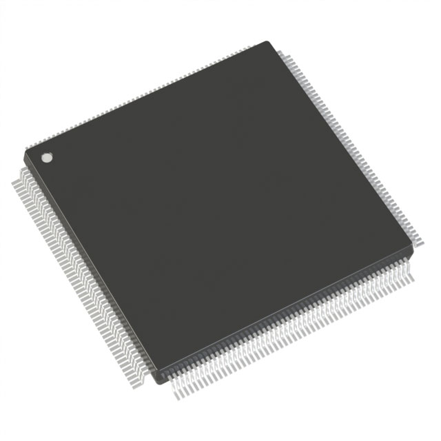
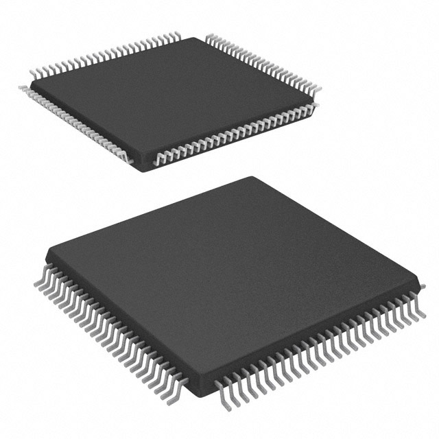
AT40K05-2AQC
| Part Description |
AT40K/KLV Field Programmable Gate Array (FPGA) IC 78 2048 256 100-TQFP |
|---|---|
| Quantity | 715 Available (as of June 15, 2026) |

| Product Category | Field Programmable Gate Array (FPGA) |
|---|---|
| Manufacturer | Microchip Technology |
| Manufacturing Status | Obsolete |
| Manufacturer Standard Lead Time | Contact Us |
| Datasheet |
Specifications & Environmental
| Device Package | 100-TQFP (14x14) | Grade | Commercial | Operating Temperature | 0°C – 70°C | ||
|---|---|---|---|---|---|---|---|
| Package / Case | 100-TQFP | Number of I/O | 78 | Voltage | 4.75 V - 5.25 V | ||
| Mounting Method | Surface Mount | RoHS Compliance | RoHS non-compliant | REACH Compliance | REACH Unaffected | ||
| Moisture Sensitivity Level | 3 (168 Hours) | Number of LABs/CLBs | 256 | Number of Logic Elements/Cells | 256 | ||
| Number of Gates | 10000 | ECCN | 3A991D | HTS Code | 8542.39.0001 | ||
| Qualification | N/A | Total RAM Bits | 2048 |
Overview of AT40K05-2AQC – AT40K FPGA, 5 V, 100‑TQFP, 78 I/O
The AT40K05-2AQC is an SRAM-based Field Programmable Gate Array (FPGA) in the AT40K family optimized for mid‑range logic and embedded memory needs. This surface-mount device provides 256 logic elements, approximately 2,048 bits of distributed on‑chip SRAM, and 78 user I/O pins in a 100‑TQFP (14×14 mm) package. Typical use cases include DSP coprocessing, custom peripheral bridging, and mid‑density logic integration where reprogrammability and on‑chip RAM are important.
Key Features
- Core Logic 256 logic elements (cells) supporting up to 10,000 usable gates for implementing custom logic, state machines, and control functions.
- Distributed SRAM (FreeRAM) Approximately 0.002 Mbits (2,048 bits) of on‑chip, 10 ns distributed SRAM enabling single/dual-port, synchronous or asynchronous memory configurations independent of logic cells.
- High Performance Primitives Series features include array multipliers and fast multiplier support; the family targets system speeds up to 100 MHz and array multiplier performance above 50 MHz.
- I/O and PCI Compatibility 78 I/O pins with 3 V/5 V capable signaling and programmable output drive; family-level documentation references PCI‑compliant I/O architectures and pin‑compatible package options.
- Clocking Family architecture includes multiple global clock resources for low‑skew distribution and flexible clock control (family supports up to 8 global clocks at series level).
- Package and Mounting 100‑TQFP (14×14 mm) surface-mount package suitable for compact PCB layouts and automated assembly.
- Power and Temperature Supply voltage range 4.75 V to 5.25 V and commercial operating temperature range of 0 °C to 70 °C.
- Compliance RoHS compliant.
- Configurable Cell Behavior Family-level features include internal tri‑state capability per cell and support for partial/complete in‑system reconfiguration workflows.
Typical Applications
- DSP Coprocessing Implement fixed‑point FIR filters, FFT stages, and arithmetic accelerators using on‑chip SRAM and array multiplier primitives.
- Custom Peripherals and Interfaces Bridge between processors and external peripherals or implement custom protocol adapters using the device’s 78 programmable I/Os.
- Embedded Control and State Machines Integrate mid‑density control logic and sequencing functions in industrial or commercial electronic systems within the specified operating range.
- Prototyping and In‑System Reconfiguration Use the device’s reprogrammability to iterate hardware‑accelerated functions or update algorithms in the field.
Unique Advantages
- Balanced Logic and Memory: A mix of 256 logic elements and 2,048 bits of distributed SRAM enables both control logic and local data buffering without external memory.
- Reprogrammability: In‑system reconfiguration capability supports design updates and adaptive functionality without replacing hardware.
- Compact, Surface‑Mount Package: 100‑TQFP (14×14) offers a space‑efficient form factor compatible with automated assembly processes.
- Clear Electrical Envelope: Defined 5 V supply range (4.75 V to 5.25 V) and commercial temperature rating simplify BOM and thermal planning for mainstream applications.
- RoHS Compliant: Meets lead‑free environmental requirements for modern electronics manufacturing.
Why Choose AT40K05-2AQC?
The AT40K05-2AQC delivers a practical combination of reprogrammable logic, embedded SRAM, and a moderate I/O count in a compact 100‑TQFP package. It is well suited for designers who need mid‑density gate capacity with on‑chip memory for DSP tasks, peripheral interfacing, or control logic within commercial temperature and 5 V power constraints. Backed by the AT40K family’s array of clocking and memory features, this device provides a stable platform for designs that require field updates and local data storage without adding external SRAM or complex board-level components.
Request a quote or submit an inquiry to purchase the AT40K05-2AQC and include your required quantities and delivery needs for a prompt response.


Date Founded: 1989
Headquarters: Chandler, Arizona, USA
Employees: 22,000+
Revenue: $8.349 Billion
Certifications and Memberships: ISO9001:2015, IATF16949:2016, AS 9100D


