
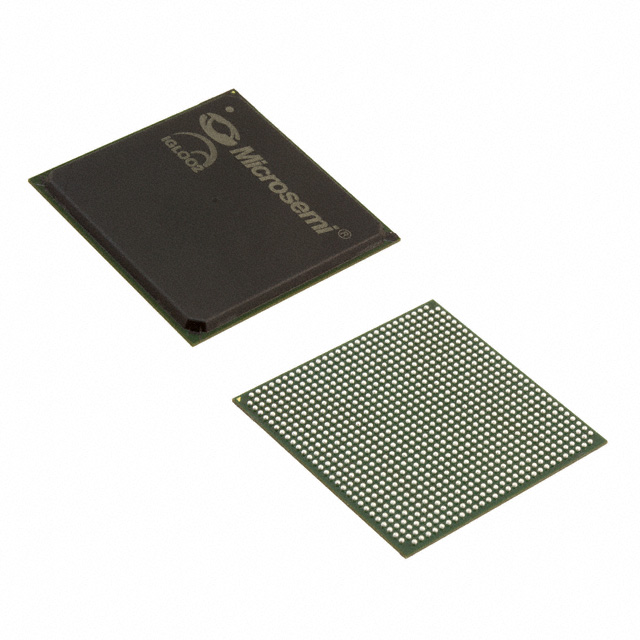
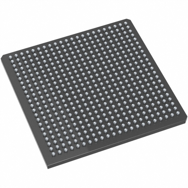
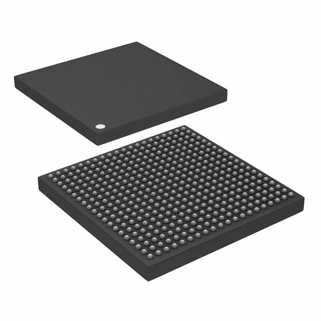
M2GL050TS-1FGG896I
| Part Description |
IGLOO2 Field Programmable Gate Array (FPGA) IC 377 1869824 56340 896-BGA |
|---|---|
| Quantity | 372 Available (as of June 18, 2026) |

| Product Category | Field Programmable Gate Array (FPGA) |
|---|---|
| Manufacturer | Microchip Technology |
| Manufacturing Status | Active |
| Manufacturer Standard Lead Time | 16 Weeks |
| Datasheet |
Specifications & Environmental
| Device Package | 896-FBGA (31x31) | Grade | Industrial | Operating Temperature | -40°C – 100°C | ||
|---|---|---|---|---|---|---|---|
| Package / Case | 896-BGA | Number of I/O | 377 | Voltage | 1.14 V - 2.625 V | ||
| Mounting Method | Surface Mount | RoHS Compliance | ROHS3 Compliant | REACH Compliance | REACH Unaffected | ||
| Moisture Sensitivity Level | 3 (168 Hours) | Number of LABs/CLBs | 56340 | Number of Logic Elements/Cells | 56340 | ||
| Number of Gates | N/A | ECCN | 5A002A1 | HTS Code | 8542.39.0001 | ||
| Qualification | N/A | Total RAM Bits | 1869824 |
Overview of M2GL050TS-1FGG896I – IGLOO2 Field Programmable Gate Array (FPGA) IC 377 1869824 56340 896-BGA
The M2GL050TS-1FGG896I is an IGLOO2 flash-based FPGA from Microchip Technology that combines programmable logic fabric with integrated high-performance communications and memory interfaces. It delivers a balance of logic density, embedded memory, and serial/memory interface capability for system designs that require configurable hardware and on-chip resources.
Built for industrial applications, the device provides 56,340 logic elements, 377 user I/Os, and approximately 1.87 Mbits of on-chip RAM, in a 896-ball BGA package (896-FBGA, 31 × 31 mm). Supply and environmental operating ranges support industrial deployment with a 1.14 V to 2.625 V supply window and an operating temperature range of −40 °C to 100 °C.
Key Features
- Flash-based FPGA fabric Fourth-generation flash-based architecture with efficient 4-input LUTs and carry chains for high-performance, reprogrammable logic.
- Logic density 56,340 logic elements to implement complex control, interface, and processing functions on-chip.
- Embedded memory Approximately 1.87 Mbits of total RAM bits, plus 64 KB embedded SRAM and up to 512 KB embedded nonvolatile memory for configuration and data buffering.
- DSP resources Up to 240 Fast Mathblocks providing 18 × 18 signed multiplication (and other multiply/accumulate capabilities) for signal processing and DSP tasks.
- High-speed serial interfaces Support for up to 16 SERDES lanes and protocol support options including PCI Express endpoint (x1/x2/x4) and XGXS/XAUI extensions for 10 Gbps class interfaces.
- High-speed memory controllers Up to two DDRx memory controllers supporting LPDDR/DDR2/DDR3 with a maximum 333 MHz clock rate and multiple DRAM bus-width modes.
- Clocking resources Multiple on-chip oscillators and up to eight Clock Conditioning Circuits (CCCs) with integrated analog PLLs; input frequency range 1–200 MHz, output 20–400 MHz.
- Security features Design security features available on all devices (encrypted bitstream loading, device certificates, anti-tamper/zeroization). Data security functions such as AES-256, SHA-256, ECC engine and PUF key enrolment are available on premium devices.
- Package and I/O 896-ball FBGA package (31 × 31 mm), 377 user I/Os, surface-mount mounting for compact board-level integration.
- Industrial operating range Rated for −40 °C to 100 °C operation and a wide supply range of 1.14 V to 2.625 V for industrial system compatibility.
Typical Applications
- High‑speed networking and switching — Use the built-in SERDES lanes and PCIe support to implement packet processing, PHY interfaces, and board-level networking functions.
- Memory subsystem and buffering — DDRx controllers and on-chip SRAM/eNVM enable memory interfacing, buffering, and data path acceleration for systems requiring external DRAM support.
- Signal processing and DSP — Mathblocks and the FPGA fabric provide hardware-accelerated multiply/accumulate and filtering workloads for industrial signal conditioning and sensor processing.
- Secure embedded systems — On-device design security and available cryptographic engines support encrypted bitstreams, secure boot, and cryptographic services where IP protection and data integrity are required.
- Industrial control and automation — Robust I/O counts, industrial temperature rating, and flexible I/O standards make the device suitable for control, interface aggregation, and deterministic logic tasks.
Unique Advantages
- Highly integrated resources: Logic elements, embedded SRAM/eNVM and dedicated mathblocks reduce external component count and simplify board designs.
- Flexible high-speed connectivity: Up to 16 SERDES lanes and PCIe endpoint capability enable direct implementation of modern serial protocols without heavy external PHY requirements.
- Scalable memory interfaces: Dual DDRx controllers and multiple DRAM bus-width modes let designers scale external memory bandwidth as system needs grow.
- Security options: Built-in design security features across all devices and advanced cryptographic primitives on premium devices help protect IP and data in the field.
- Industrial suitability: Wide supply range, surface-mount 896-FBGA package, and −40 °C to 100 °C operation support deployment in demanding environments.
- On-chip clocking and timing: Multiple oscillators and up to eight CCCs with PLLs simplify clock distribution and phase management for multi-domain designs.
Why Choose M2GL050TS-1FGG896I?
The M2GL050TS-1FGG896I IGLOO2 FPGA combines substantial logic density, embedded memory, DSP resources, and high-speed serial/memory interfaces in a single flash-based device targeted at industrial applications. Its integrated security features and flexible I/O make it suitable for designs that need reconfigurable hardware with on-chip acceleration and protected intellectual property.
Choose this device when you need a compact, industrial-grade FPGA solution that balances configurable logic, on-chip RAM and nonvolatile storage, high-speed connectivity, and clocking resources — all within an 896-FBGA package and a wide operating range for robust system deployment.
Request a quote or submit an inquiry to receive pricing and availability details for the M2GL050TS-1FGG896I.


Date Founded: 1989
Headquarters: Chandler, Arizona, USA
Employees: 22,000+
Revenue: $8.349 Billion
Certifications and Memberships: ISO9001:2015, IATF16949:2016, AS 9100D


