IS42S32400B-6B
| Part Description |
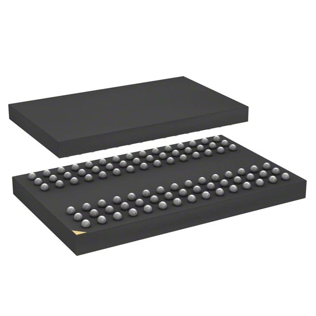
IC DRAM 128MBIT PAR 90TFBGA |
|---|---|
| Quantity | 1,680 Available (as of June 13, 2026) |

| Product Category | Memory |
|---|---|
| Manufacturer | Integrated Silicon Solution Inc |
| Manufacturing Status | Obsolete |
| Manufacturer Standard Lead Time | Contact Us |
| Datasheet |
Specifications & Environmental
| Device Package | 90-TFBGA (8x13) | Memory Format | DRAM | Technology | SDRAM | ||
|---|---|---|---|---|---|---|---|
| Memory Size | 128 Mbit | Access Time | 5.4 ns | Grade | Commercial | ||
| Clock Frequency | 166 MHz | Voltage | 3V ~ 3.6V | Memory Type | Volatile | ||
| Operating Temperature | 0°C ~ 70°C (TA) | Write Cycle Time Word Page | N/A | Packaging | 90-TFBGA | ||
| Mounting Method | Volatile | Memory Interface | Parallel | Memory Organization | 4M x 32 | ||
| Moisture Sensitivity Level | 3 (168 Hours) | RoHS Compliance | ROHS3 Compliant | REACH Compliance | REACH Unaffected | ||
| Qualification | N/A | ECCN | EAR99 | HTS Code | 8542.32.0002 |
Overview of IS42S32400B-6B – IC DRAM 128MBIT PAR 90TFBGA
The IS42S32400B-6B is a 128‑Mbit synchronous DRAM organized as 4M × 32 with an internal quad‑bank architecture and pipeline operation. It provides synchronous, burst‑oriented parallel memory access with programmable burst length and CAS latency for high‑speed data transfer.
This device targets designs that require a parallel SDRAM solution with selectable CAS latency, bank interleaving and self‑refresh capabilities. Key value propositions include support for up to 166 MHz clock operation, flexible burst modes, and a compact 90‑TFBGA (8×13) package.
Key Features
- Memory Organization — 128 Mbit total capacity organized as 4M × 32 with four internal banks (1M × 32 × 4), enabling bank interleaving and random column access every clock cycle.
- Synchronous SDRAM Core — Fully synchronous operation with all signals referenced to the rising edge of the clock and pipeline architecture for high‑speed transfers.
- Clock and Timing — Supports clock frequencies up to 166 MHz (device speed grade -6); programmable CAS latency options of 2 or 3 clocks with access time from clock as low as 5.4 ns at CAS‑3.
- Burst and Access Control — Programmable burst lengths (1, 2, 4, 8, full page) and burst sequences (sequential/interleave); burst read/write and burst read/single write operations with burst termination commands.
- Refresh and Power Management — Auto Refresh and Self Refresh modes with 4096 refresh cycles every 64 ms; includes power‑down functionality.
- Interface and Logic Levels — LVTTL compatible inputs/outputs and parallel memory interface for standard SDRAM control.
- Power Supply — Voltage supply range specified as 3.0 V to 3.6 V; datasheet lists VDD and VDDQ at 3.3 V.
- Package and Temperature — Supplied in a 90‑TFBGA (8×13) package; operating temperature range 0°C to 70°C (TA).
Typical Applications
- High‑speed data buffering — Use where synchronous, burst‑oriented parallel transfers and low access latency are required.
- System memory in embedded platforms — Fits designs requiring a parallel SDRAM with programmable CAS latency and bank interleaving.
- Temporary data storage for pipeline architectures — Supports burst read/write sequences and random column access for pipelined data flows.
Unique Advantages
- Programmable performance profile: Selectable CAS latency (2 or 3) and multiple clock frequency grades (up to 166 MHz) to match system timing requirements.
- Flexible burst control: Programmable burst lengths and sequences allow tuning of transfer patterns for different access behaviors.
- Bank interleaving for throughput: Quad‑bank internal architecture enables precharge hiding and improved effective throughput during random accesses.
- Power and refresh modes: Auto Refresh, Self Refresh and power‑down modes help manage power during idle intervals while maintaining data integrity.
- Compact BGA package: 90‑TFBGA (8×13) provides a dense, solderable footprint suitable for space‑constrained PCB designs.
Why Choose IS42S32400B-6B?
The IS42S32400B-6B combines a synchronous, pipeline SDRAM architecture with programmable timing and burst controls to deliver configurable high‑speed parallel memory. Its quad‑bank organization and support for up to 166 MHz operation make it suitable for designs that require low‑latency burst transfers and flexible access patterns.
This device is appropriate for engineers specifying a 128 Mbit SDRAM in a compact 90‑TFBGA package with 3.0–3.6 V supply operation and standard LVTTL signaling. Backed by manufacturer documentation and defined timing parameters, it provides a verifiable component choice for systems needing synchronous DRAM functionality.
Request a quote or submit a sales inquiry to receive pricing, availability and extended support information for IS42S32400B-6B.