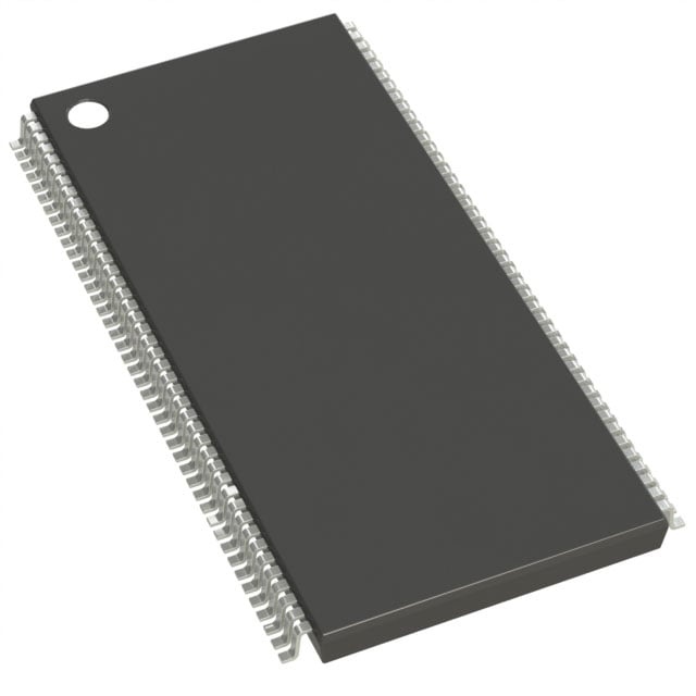
IS42S32400B-6TL
| Part Description |
IC DRAM 128MBIT PAR 86TSOP II |
|---|---|
| Quantity | 440 Available (as of June 14, 2026) |

| Product Category | Memory |
|---|---|
| Manufacturer | Integrated Silicon Solution Inc |
| Manufacturing Status | Obsolete |
| Manufacturer Standard Lead Time | Contact Us |
| Datasheet |
Specifications & Environmental
| Device Package | 86-TSOP II | Memory Format | DRAM | Technology | SDRAM | ||
|---|---|---|---|---|---|---|---|
| Memory Size | 128 Mbit | Access Time | 5.4 ns | Grade | Commercial | ||
| Clock Frequency | 166 MHz | Voltage | 3V ~ 3.6V | Memory Type | Volatile | ||
| Operating Temperature | 0°C ~ 70°C (TA) | Write Cycle Time Word Page | N/A | Packaging | 86-TFSOP (0.400", 10.16mm Width) | ||
| Mounting Method | Volatile | Memory Interface | Parallel | Memory Organization | 4M x 32 | ||
| Moisture Sensitivity Level | 3 (168 Hours) | RoHS Compliance | ROHS Compliant | REACH Compliance | REACH Unaffected | ||
| Qualification | N/A | ECCN | EAR99 | HTS Code | 8542.32.0002 |
Overview of IS42S32400B-6TL – 128Mbit Synchronous DRAM (86‑TSOP II)
The IS42S32400B-6TL is a 128‑Mbit synchronous DRAM organized as 4M × 32 with a quad‑bank architecture and fully synchronous, clocked operation. It implements a pipeline architecture with registered inputs and outputs for predictable timing and high‑speed burst transfers.
Targeted for systems that require a parallel SDRAM interface, the device supports up to 166 MHz clock operation (CAS latency = 3) and offers programmable burst lengths, auto/self refresh modes, and LVTTL signaling on a 3.3 V supply range.
Key Features
- Core / Memory Organization 128 Mbit density configured internally as 4M × 32 across four banks for concurrent access and bank interleaving.
- Performance Supports clock frequencies up to 166 MHz (CAS latency = 3) with an access time from clock of 5.4 ns (CAS = 3); programmable CAS latency of 2 or 3 clocks.
- Burst and Sequencing Programmable burst lengths (1, 2, 4, 8, full page) and selectable sequential or interleaved burst sequences; burst termination through burst stop and auto precharge.
- Refresh and Power Modes Auto Refresh (CBR) and Self Refresh with programmable refresh periods; 4096 refresh cycles every 64 ms to maintain data integrity.
- Interface and Signaling LVTTL‑compatible parallel interface with registered inputs and outputs referenced to the rising clock edge for synchronous operation.
- Power Designed for 3.0 V to 3.6 V supplies (VDD / VDDQ = 3.3 V typical as specified).
- Package and Temperature Supplied in an 86‑pin TSOP‑II package (86‑TFSOP, 0.400", 10.16 mm width); specified operating temperature 0 °C to 70 °C (TA).
Typical Applications
- Parallel memory subsystems — Provides 128 Mbit of synchronous DRAM in a 4M × 32 organization suitable for designs that require a parallel SDRAM interface and predictable burst transfers.
- High‑speed buffering — Up to 166 MHz clock operation and programmable burst lengths support high‑throughput buffer and temporary storage roles in digital systems.
- Embedded systems — LVTTL interface and 3.3 V supply range make the device suitable for embedded designs needing mid‑density DRAM in an 86‑pin TSOP‑II footprint.
Unique Advantages
- Quad‑bank architecture for hidden precharge: Internal bank structure enables interleaving to hide row precharge time and maintain continuous data flow during burst operations.
- Flexible burst control: Programmable burst lengths and sequence options allow tailoring transfer patterns to system memory access requirements.
- Programmable CAS latency: Support for CAS = 2 or 3 lets designers balance latency and maximum clock frequency (up to 166 MHz at CAS = 3).
- Comprehensive refresh modes: Auto and self refresh with defined refresh cycles (4096 every 64 ms) help preserve data with predictable timing behavior.
- Standard TSOP‑II footprint: 86‑pin TSOP‑II package simplifies board placement in designs constrained to that common form factor and 10.16 mm width.
Why Choose IS42S32400B-6TL?
The IS42S32400B-6TL delivers a balanced combination of mid‑density storage, synchronous parallel interface, and programmable timing features for systems that require deterministic burst transfers and bank‑interleaved access. With support for up to 166 MHz operation, programmable CAS latency, and robust refresh options, it fits designs that need reliable, high‑throughput DRAM in an 86‑pin TSOP‑II package.
This device is suitable for engineers specifying a 128 Mbit SDRAM with LVTTL signaling and a 3.0–3.6 V supply window, offering clear, verifiable timing and refresh behavior for long‑lived designs.
If you need pricing, availability, or a formal quote for the IS42S32400B-6TL, submit a request for a quote or contact sales to obtain current lead times and ordering information.