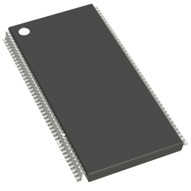
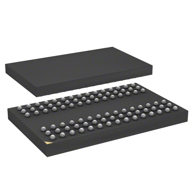
IS42S32400B-7B
| Part Description |
IC DRAM 128MBIT PAR 90TFBGA |
|---|---|
| Quantity | 583 Available (as of June 15, 2026) |
| Product Category | Memory |
|---|---|
| Manufacturer | Integrated Silicon Solution Inc |
| Manufacturing Status | Obsolete |
| Manufacturer Standard Lead Time | Contact Us |
| Datasheet |
Specifications & Environmental
| Device Package | 90-TFBGA (8x13) | Memory Format | DRAM | Technology | SDRAM | ||
|---|---|---|---|---|---|---|---|
| Memory Size | 128 Mbit | Access Time | 5.4 ns | Grade | Commercial | ||
| Clock Frequency | 143 MHz | Voltage | 3V ~ 3.6V | Memory Type | Volatile | ||
| Operating Temperature | 0°C ~ 70°C (TA) | Write Cycle Time Word Page | N/A | Packaging | 90-TFBGA | ||
| Mounting Method | Volatile | Memory Interface | Parallel | Memory Organization | 4M x 32 | ||
| Moisture Sensitivity Level | 3 (168 Hours) | RoHS Compliance | ROHS3 Compliant | REACH Compliance | REACH Unaffected | ||
| Qualification | N/A | ECCN | EAR99 | HTS Code | 8542.32.0002 |
Overview of IS42S32400B-7B – IC DRAM 128MBIT PAR 90TFBGA
The IS42S32400B-7B is a 128‑Mbit synchronous DRAM organized as 4M × 32 with an internal quad‑bank architecture and pipeline design for high‑speed synchronous operation. The device provides programmable burst operation, selectable CAS latency, and refresh management for use in systems requiring parallel SDRAM memory in a compact 90‑TFBGA package.
Designed for applications that need a 128 Mbit parallel SDRAM with deterministic timing and burst access, the IS42S32400B-7B delivers selectable performance and system-level refresh features while operating within the specified voltage and temperature ranges.
Key Features
- Memory Architecture 128‑Mbit SDRAM organized as 4M × 32 with four internal banks to support interleaved access and hide row precharge latency.
- Synchronous Pipeline Operation Fully synchronous interface with all signals referenced to the rising edge of CLK for predictable timing in burst transfers.
- Performance Options Clock frequency support includes 143 MHz (device specification); programmable CAS latency options of 2 or 3 clocks and an access time from clock of 5.4 ns (CAS‑3).
- Burst and Sequencing Programmable burst lengths (1, 2, 4, 8, full page) and selectable burst sequence (sequential/interleave) for flexible block transfers.
- Refresh and Power Modes Auto Refresh and Self Refresh support with 4096 refresh cycles every 64 ms and programmable refresh periods for memory integrity and power management.
- Interface LVTTL compatible inputs/outputs and a parallel memory interface suitable for synchronous system designs.
- Power Supply voltage range specified as 3.0 V to 3.6 V (VDD / VDDQ), supporting standard 3.3 V memory systems.
- Package & Temperature Supplied in a 90‑TFBGA (8 × 13) package; operating ambient temperature range specified as 0°C to 70°C (TA).
Typical Applications
- Embedded memory subsystems Provides a 128‑Mbit parallel SDRAM option in space‑constrained boards where a 90‑TFBGA footprint is required.
- High‑throughput buffering Programmable burst lengths and synchronous operation enable efficient block transfers for buffering and frame storage.
- System memory for industrial designs Support for Auto Refresh and Self Refresh helps maintain data integrity in long‑running systems within the specified temperature range.
Unique Advantages
- Flexible timing configuration: Programmable CAS latency (2 or 3) and selectable burst settings allow optimization for throughput and latency tradeoffs.
- Quad‑bank architecture: Internal banking and interleaving capability enable overlapping of row operations to reduce effective access overhead.
- Deterministic synchronous interface: All inputs and outputs referenced to CLK simplify timing analysis and integration into synchronous memory systems.
- Comprehensive refresh control: Auto and Self Refresh modes with defined refresh cycles (4096/64 ms) support reliable long‑term data retention.
- Compact package: 90‑TFBGA (8×13) offers a reduced PCB footprint for dense designs requiring parallel SDRAM.
Why Choose IC DRAM 128MBIT PAR 90TFBGA?
The IS42S32400B-7B combines a synchronous pipeline architecture, programmable burst and latency options, and internal quad‑bank design to deliver controllable high‑speed SDRAM behavior for parallel memory systems. Its supply voltage range and LVTTL interface make it compatible with standard 3.3 V memory platforms, while built‑in refresh and power modes support robust operation.
This device is ideal for designers who need a 128‑Mbit parallel SDRAM in a compact 90‑TFBGA package and require explicit, verifiable timing control and refresh management. The documented performance parameters and configuration options support predictable integration into embedded and system memory designs.
Request a quote or submit a request for availability and pricing for the IS42S32400B-7B to discuss lead times and volume options.