IS42S32400B-7BLI
| Part Description |
IC DRAM 128MBIT PAR 90TFBGA |
|---|---|
| Quantity | 7 Available (as of June 15, 2026) |

| Product Category | Memory |
|---|---|
| Manufacturer | Integrated Silicon Solution Inc |
| Manufacturing Status | Obsolete |
| Manufacturer Standard Lead Time | Contact Us |
| Datasheet |
Specifications & Environmental
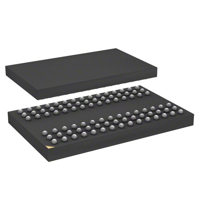
| Device Package | 90-TFBGA (8x13) | Memory Format | DRAM | Technology | SDRAM | ||
|---|---|---|---|---|---|---|---|
| Memory Size | 128 Mbit | Access Time | 5.4 ns | Grade | Industrial | ||
| Clock Frequency | 143 MHz | Voltage | 3V ~ 3.6V | Memory Type | Volatile | ||
| Operating Temperature | -40°C ~ 85°C (TA) | Write Cycle Time Word Page | N/A | Packaging | 90-TFBGA | ||
| Mounting Method | Volatile | Memory Interface | Parallel | Memory Organization | 4M x 32 | ||
| Moisture Sensitivity Level | 3 (168 Hours) | RoHS Compliance | ROHS3 Compliant | REACH Compliance | REACH Unaffected | ||
| Qualification | N/A | ECCN | EAR99 | HTS Code | 8542.32.0002 |
Overview of IS42S32400B-7BLI – IC DRAM 128MBIT PAR 90TFBGA
The IS42S32400B-7BLI is a 128‑Mbit synchronous DRAM (SDRAM) organized as 4M × 32 with a quad‑bank architecture and pipeline synchronous interface. It provides high‑speed burst read/write operation with programmable burst lengths and CAS latency options to support time‑sensitive memory access patterns.
This device targets systems that require a compact 90‑TFBGA package, operation from a nominal 3.3V supply (VDD/VDDQ) within a 3.0–3.6V range, and industrial temperature operation down to −40°C. Key value propositions include synchronous high‑speed transfer, flexible burst and refresh control, and a compact ball‑grid package for space‑constrained designs.
Key Features
- Memory Organization The device is organized as 4M × 32 bits for a total of 128 Mbit with four internal banks (each 33,554,432 bits).
- Synchronous SDRAM Core Fully synchronous operation with all signals referenced to the rising edge of CLK and LVTTL‑compatible inputs/outputs.
- Performance Supports clock frequencies including 143 MHz (‑7 speed grade) and access times as low as 5.4 ns (CAS‑latency = 3).
- Programmable Burst & Latency Programmable burst lengths (1, 2, 4, 8, full page), sequential/interleave burst sequencing, and selectable CAS latency (2 or 3 clocks).
- Refresh & Power Modes Auto Refresh (CBR), Self Refresh with programmable refresh periods, and 4096 refresh cycles every 64 ms.
- Voltage & Interface Nominal VDD/VDDQ 3.3V operation with allowable supply range 3.0–3.6V; parallel memory interface with LVTTL signals.
- Package & Temperature Supplied in a 90‑TFBGA (8×13) package and available in an industrial temperature range of −40°C to 85°C.
- Compliance Options Device is available in lead‑free packages.
Typical Applications
- Embedded systems Use as on‑board SDRAM where 128 Mbit capacity and synchronous burst operation support program and data buffering.
- Industrial equipment Industrial temperature availability (−40°C to 85°C) makes the device suitable for factory and field electronics requiring robust memory.
- High‑speed data buffering Pipeline synchronous architecture and programmable burst behavior support designs needing predictable, high‑rate data transfer.
Unique Advantages
- Synchronous pipeline architecture: Enables high‑speed data transfers with all I/O referenced to the clock edge for predictable timing.
- Flexible burst and latency control: Programmable burst lengths and CAS latency options let designers optimize throughput and latency for specific access patterns.
- Bank interleaving and auto‑precharge: Internal bank structure and auto/precharge features hide row access time and improve effective random access performance.
- Industrial temperature support: Operation from −40°C to 85°C addresses temperature‑sensitive applications without requiring additional derating.
- Compact 90‑TFBGA package: 8×13 ball‑grid footprint provides a high density solution for space‑constrained PCBs.
- Standard 3.3V supply compatibility: Nominal VDD/VDDQ of 3.3V with an allowed supply range of 3.0–3.6V simplifies integration into common system power architectures.
Why Choose IS42S32400B-7BLI?
The IS42S32400B-7BLI delivers a practical balance of capacity, speed, and configurability for designs requiring 128 Mbit of synchronous DRAM in a compact FBGA package. Its programmable burst modes, selectable CAS latencies, and internal bank architecture support efficient, high‑throughput memory access patterns while the industrial temperature option and lead‑free availability address demanding deployment environments.
This device is well suited to engineers specifying synchronous parallel DRAM for embedded platforms, industrial controllers, and other systems needing deterministic, burst‑oriented memory behavior with a small PCB footprint.
Request a quote or submit an inquiry to receive pricing, availability, and lead‑time information for the IS42S32400B-7BLI.