IS42S32400B-7T
| Part Description |
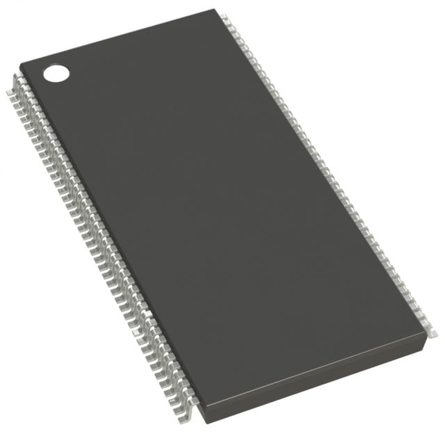
IC DRAM 128MBIT PAR 86TSOP II |
|---|---|
| Quantity | 1,586 Available (as of June 11, 2026) |

| Product Category | Memory |
|---|---|
| Manufacturer | Integrated Silicon Solution Inc |
| Manufacturing Status | Obsolete |
| Manufacturer Standard Lead Time | Contact Us |
| Datasheet |
Specifications & Environmental
| Device Package | 86-TSOP II | Memory Format | DRAM | Technology | SDRAM | ||
|---|---|---|---|---|---|---|---|
| Memory Size | 128 Mbit | Access Time | 5.4 ns | Grade | Commercial | ||
| Clock Frequency | 143 MHz | Voltage | 3V ~ 3.6V | Memory Type | Volatile | ||
| Operating Temperature | 0°C ~ 70°C (TA) | Write Cycle Time Word Page | N/A | Packaging | 86-TFSOP (0.400", 10.16mm Width) | ||
| Mounting Method | Volatile | Memory Interface | Parallel | Memory Organization | 4M x 32 | ||
| Moisture Sensitivity Level | 3 (168 Hours) | RoHS Compliance | ROHS Compliant | REACH Compliance | REACH Unaffected | ||
| Qualification | N/A | ECCN | EAR99 | HTS Code | 8542.32.0002 |
Overview of IS42S32400B-7T – IC DRAM 128MBIT PAR 86TSOP II
The IS42S32400B-7T is a 128‑Mbit synchronous DRAM organized as 4M × 32 with a parallel memory interface. It implements a quad‑bank, fully synchronous pipeline architecture with registered inputs and outputs referenced to the rising edge of CLK.
Designed for systems requiring programmable burst operation and high‑speed synchronous transfers, the device delivers flexible timing (programmable CAS latency and burst lengths), automatic refresh modes, and a compact 86‑pin TSOP‑II package suitable for commercial temperature operation (0°C to 70°C).
Key Features
- Memory Architecture 128 Mbit organized as 4M × 32 with four internal banks to enable interleaving and hide row precharge latency.
- High‑speed Synchronous Operation Clock frequency (‑7) rating at 143 MHz with fully synchronous signaling and LVTTL compatible inputs/outputs.
- Programmable Timing Selectable CAS latency (2 or 3 clocks) and programmable burst lengths (1, 2, 4, 8, full page) with sequential or interleave burst sequencing.
- Performance / Access Time Access time from clock of 5.4 ns at CAS latency = 3 (per device timing tables).
- Refresh and Power Modes Auto Refresh (including CBR), Self Refresh with programmable refresh periods, and 4096 refresh cycles every 64 ms for data retention management.
- Voltage Single supply operation within 3.0 V to 3.6 V.
- Package and Mounting Available in an 86‑pin TSOP‑II (86‑TFSOP, 0.400", 10.16 mm width) package; also offered in alternate package options per device family.
- Manufacturing Options Device family notes availability in industrial temperature ranges and lead‑free variants (per datasheet options).
Typical Applications
- High‑speed data buffering Use where synchronous burst transfers and random column access are needed for short latency buffering and streaming.
- System memory expansion Parallel SDRAM capacity for designs that require 128 Mbit memory organized as 4M × 32 with programmable burst behavior.
- Embedded and commercial electronics Commercial temperature (0°C to 70°C) systems benefiting from low‑latency, burst‑oriented DRAM access and LVTTL signaling.
Unique Advantages
- Flexible timing configuration: Programmable CAS latency and burst lengths let designers tune latency and throughput to match system timing requirements.
- Quad‑bank interleaving: Internal bank architecture enables precharging of one bank while accessing another to reduce effective access gaps.
- Comprehensive refresh control: Auto Refresh, Self Refresh and 4096 refresh cycles every 64 ms provide deterministic retention management for synchronous systems.
- Compact board footprint: 86‑pin TSOP‑II package (10.16 mm width) offers a dense solution for space‑constrained PCB layouts.
- Voltage compatibility: 3.0 V to 3.6 V supply range supports common 3.3 V memory system rails.
Why Choose IS42S32400B-7T?
The IS42S32400B-7T combines a 128‑Mbit SDRAM organization with programmable timing and banked architecture to deliver flexible, high‑speed synchronous memory for commercial systems. Its LVTTL interface, selectable CAS latency, and programmable burst options let engineers optimize latency and throughput for a range of burst‑oriented memory tasks.
With support for automatic and self refresh, a defined commercial operating temperature range, and compact 86‑pin TSOP‑II packaging, the device is suited to designs that require verified synchronous DRAM behavior, predictable refresh management, and a small PCB footprint.
Request a quote or submit an inquiry to obtain pricing, lead times, and availability for the IS42S32400B-7T. Provide part number and required quantity for a prompt response.