IS42S32400B-7TL
| Part Description |
IC DRAM 128MBIT PAR 86TSOP II |
|---|---|
| Quantity | 806 Available (as of June 12, 2026) |

| Product Category | Memory |
|---|---|
| Manufacturer | Integrated Silicon Solution Inc |
| Manufacturing Status | Obsolete |
| Manufacturer Standard Lead Time | Contact Us |
| Datasheet |
Specifications & Environmental
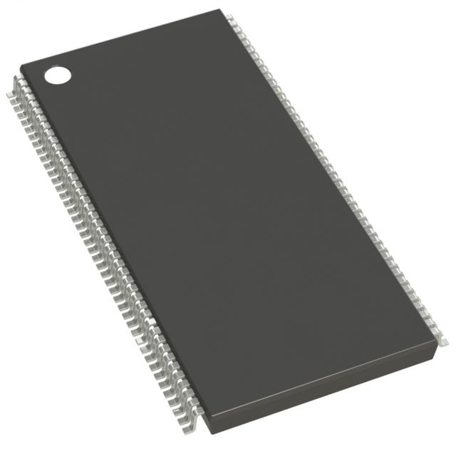
| Device Package | 86-TSOP II | Memory Format | DRAM | Technology | SDRAM | ||
|---|---|---|---|---|---|---|---|
| Memory Size | 128 Mbit | Access Time | 5.4 ns | Grade | Commercial | ||
| Clock Frequency | 143 MHz | Voltage | 3V ~ 3.6V | Memory Type | Volatile | ||
| Operating Temperature | 0°C ~ 70°C (TA) | Write Cycle Time Word Page | N/A | Packaging | 86-TFSOP (0.400", 10.16mm Width) | ||
| Mounting Method | Volatile | Memory Interface | Parallel | Memory Organization | 4M x 32 | ||
| Moisture Sensitivity Level | 3 (168 Hours) | RoHS Compliance | ROHS3 Compliant | REACH Compliance | REACH Unaffected | ||
| Qualification | N/A | ECCN | EAR99 | HTS Code | 8542.32.0002 |
Overview of IS42S32400B-7TL – IC DRAM 128MBIT PAR 86TSOP II
The IS42S32400B-7TL is a 128‑Mbit synchronous DRAM (SDRAM) organized as 4M × 32 with a quad‑bank architecture and pipeline data path. Manufactured by Integrated Silicon Solution, Inc. (ISSI), this part provides a parallel, fully synchronous memory interface suitable for high‑speed burst transfers and memory subsystems.
Designed for systems requiring programmable burst operation and low‑latency access, the device supports high clock rates and a range of refresh and power‑down modes to balance performance and system power management.
Key Features
- Memory Architecture 128 Mbit SDRAM organized as 4M × 32 with four internal banks and internal row/column organization (4,096 rows × 256 columns × 32 bits).
- Performance & Timing –7 speed grade supports up to 143 MHz clock with an access time from clock of 5.4 ns (CAS latency = 3); programmable CAS latency options of 2 or 3 clocks.
- Burst and Access Modes Programmable burst lengths (1, 2, 4, 8, full page) and burst sequences (sequential/interleave). Supports burst read/write and burst read/single write operations with burst termination and auto precharge capability.
- Refresh & Power Management Auto Refresh (CBR) and Self Refresh with programmable refresh periods; 4096 refresh cycles every 64 ms. Includes power‑down and self‑timed precharge features to manage power and timing.
- Interface Fully synchronous interface with all signals referenced to the rising edge of CLK and LVTTL‑compatible inputs/outputs for parallel memory systems.
- Voltage Specified supply range 3.0 V to 3.6 V; device defined for 3.3 V VDD/VDDQ operation.
- Package & Temperature Available in an 86‑pin TSOP‑II package (0.400" / 10.16 mm width). Standard operating temperature 0 °C to 70 °C (TA); industrial temperature versions are available.
Typical Applications
- High‑speed memory subsystems Use as parallel SDRAM storage for designs requiring synchronous burst transfers and predictable, clock‑referenced timing.
- Buffering and data staging Quad‑bank architecture and programmable burst modes enable efficient buffering and block transfers with hidden precharge cycles.
- Embedded systems with parallel interfaces LVTTL‑compatible synchronous interface and parallel data organization suit embedded designs that integrate discrete SDRAM devices.
Unique Advantages
- Flexible performance scaling Multiple speed grades (including the –7 grade at 143 MHz) and selectable CAS latencies let designers balance throughput and timing constraints.
- Programmable burst control Configurable burst lengths and sequences simplify block data transfers and support both sequential and interleaved access patterns.
- Quad‑bank memory for hidden precharge Internal banking allows precharge of one bank while accessing another, reducing effective access latency for random operations.
- Synchronous LVTTL interface All signals registered to the rising clock edge and LVTTL compatibility make timing deterministic and integration straightforward in parallel memory systems.
- Compact package options 86‑pin TSOP‑II offers a compact footprint; device is also offered in alternate package types per device family options.
- Refresh and low‑power modes Auto and self refresh, plus power‑down modes, provide control over refresh behavior and system power consumption.
Why Choose IC DRAM 128MBIT PAR 86TSOP II?
The IS42S32400B-7TL delivers a synchronous, parallel 128‑Mbit SDRAM solution that combines programmable burst operation, selectable CAS latency, and quad‑bank architecture for predictable, high‑throughput memory access. Its LVTTL interface and 3.0–3.6 V supply range make it suitable for designs that require clock‑referenced timing and parallel data paths.
This device is appropriate for engineers building memory subsystems and embedded platforms that need configurable burst behavior, low access latency, and compact packaging. Backed by ISSI datasheet specifications and available package/temperature variants, it provides a verifiable component choice for long‑term design planning and system integration.
Request a quote or submit an RFQ to check current availability and pricing for IS42S32400B-7TL.