
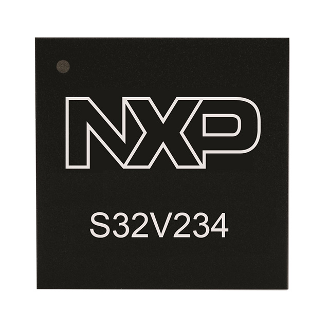
FS32V234CKN2VUB
| Part Description |
ARM® Cortex®-A53 Microprocessor IC FS32V23 4 Core, 32/64-Bit 1GHz 621-FCPBGA (17x17) |
|---|---|
| Quantity | 63 Available (as of October 8, 2026) |

| Product Category | Microprocessors |
|---|---|
| Part Series | FS32V234 |
| Manufacturer | NXP USA Inc. |
| Manufacturing Status | Active |
| Manufacturer Standard Lead Time | 52 Weeks |
| Datasheet |
Specifications & Environmental
| Co-Processors/DSP | ARM® Cortex®-M4 | Core Processor | ARM® Cortex®-A53 | Device Package | 621-FCPBGA (17x17) | ||
|---|---|---|---|---|---|---|---|
| Display & Interface Controllers | APEX2-CL, DCU (2D-ACE), ISP, LCD, MIPICSI2, Video, VIU | ECCN | N/A | Ethernet | GbE | ||
| Graphics Acceleration | No | HTS Code | N/A | Moisture Sensitivity Level | N/A | ||
| Mounting Method | Surface Mount | Mounting Type | Surface Mount | Number of Cores/Bus Width | 4 Core, 32/64-Bit | ||
| Operating Temperature | -40°C ~ 125°C (TJ) | Package / Case | 621-FBGA, FCBGA | RAM Controllers | DDR3, DDR3L, LPDDR2 | ||
| REACH Compliance | REACH Unaffected | RoHS Compliance | Unknown | Security Features | AES, ARM TZ, Boot, CSE, OCOTP_CTRL, System JTAG | ||
| Speed | 1GHz | Supplier Device Package | 621-FCPBGA (17×17) | Voltage – I/O | 1V, 1.8V, 3.3V |
Overview of FS32V234CKN2VUB – ARM® Cortex®-A53 4‑Core 1 GHz Microprocessor, 621‑FCPBGA (17×17)
The FS32V234CKN2VUB is an embedded microprocessor IC featuring a quad ARM® Cortex®‑A53 processor cluster operating up to 1 GHz and a companion ARM® Cortex®‑M4 co‑processor. It integrates memory controllers, rich video and camera interfaces, Ethernet connectivity, and hardware security primitives, making it a compact computing foundation for complex embedded systems.
Targeted at industrial and embedded applications, the device delivers a combination of multi‑core processing, image and video input capabilities, and configurable memory interfaces while supporting extended operating temperatures for demanding environments.
Key Features
- CPU Architecture — Quad ARM® Cortex®‑A53 cores (32/64‑bit) at up to 1 GHz with L1 and L2 cache architecture; includes an ARM® Cortex®‑M4 co‑processor for real‑time tasks.
- Memory and Boot — 32‑bit DRAM controller supporting DDR3, DDR3L and LPDDR2, plus QuadSPI with Execute‑In‑Place (XIP) and boot flash fault detection/correction schemes.
- Video and Imaging Interfaces — Display and image subsystem including APEX2‑CL, DCU (2D‑ACE), ISP, LCD, MIPI‑CSI2, Video and VIU blocks for camera input and image processing.
- Connectivity — Integrated Gigabit Ethernet (GbE) and additional interfaces such as I2C, UART, SPI, PCIe 2.0 (endpoint/root complex), FD‑CAN and FlexRay support referenced in the series data.
- Security — On‑chip CSE with secure RAM/ROM, ARM TrustZone support, AES boot capability, One‑Time Programmable controller (OCOTP_CTRL) and System JTAG for secure boot and device protection.
- System Reliability and Safety — ECC/parity support for memories, hardware CRC, watchdog, eDMA with DMAMUX, and documented safety measures (series data references ISO 26262 ASIL‑targeted features).
- Power and Clocking — Flexible run modes and peripheral clock gating, PLLs and multiple oscillator options to support power‑managed operation.
- Package and Temperature — 621‑FCPBGA surface‑mount package (17×17 mm) and industrial operating temperature range of −40 °C to 125 °C.
- Compliance — RoHS compliant.
Typical Applications
- Industrial Automation — Real‑time control and supervisory processing using the Cortex‑M4 for deterministic tasks and Cortex‑A53 cores for HMI and analytics.
- Vision and Imaging Systems — Camera input and image signal processing via MIPI‑CSI2, ISP and VIU blocks for machine vision and inspection systems.
- Networked Embedded Systems — GbE connectivity and protocol interfaces for industrial gateways, communication modules and distributed controllers.
- Safety‑Oriented Embedded Platforms — On‑chip safety and memory error detection features suitable for designs requiring documented safety measures.
Unique Advantages
- Balanced Multi‑Core Architecture: Combines quad Cortex‑A53 application cores with a Cortex‑M4 co‑processor to separate high‑level and real‑time workloads.
- Integrated Imaging and Display Support: Multiple display and camera interfaces reduce external component needs for vision‑centric designs.
- Robust Memory and Boot Options: Support for DDR3/DDR3L/LPDDR2 and QuadSPI XIP simplifies memory subsystem design and boot reliability through parity and fault detection schemes.
- Built‑In Security Primitives: CSE, TrustZone support, AES boot and OCOTP_CTRL provide hardware anchors for secure boot and device provisioning.
- Industrial Temperature Range: Rated for −40 °C to 125 °C to meet environmental demands of industrial deployments.
- Manufacturer Backing: Part of the NXP Semiconductors S32V234 family with documented technical data and safety resources referenced in the series documentation.
Why Choose FS32V234CKN2VUB?
FS32V234CKN2VUB positions itself as a versatile embedded compute node combining multi‑core application processing with a dedicated real‑time co‑processor, broad memory interface support, and integrated imaging and connectivity features. The package and industrial temperature range make it suitable for deployment in demanding embedded and industrial environments.
Engineers designing networked, vision‑enabled or safety‑aware systems can leverage the device’s on‑chip security and memory integrity features, plus NXP’s series documentation and technical resources, to streamline development and long‑term support.
Request a quote or submit an inquiry for FS32V234CKN2VUB to discuss availability, pricing and integration support for your design needs.




















Date Founded: 2006
Headquarters: Eindhoven, North Brabant, Netherlands
Employees: 38,000+
Revenue: $10.53 Billion
Certifications and Memberships: ISO9001:2015, IATF16949:2016


