
IDT79RC32V334-150BB
| Part Description |
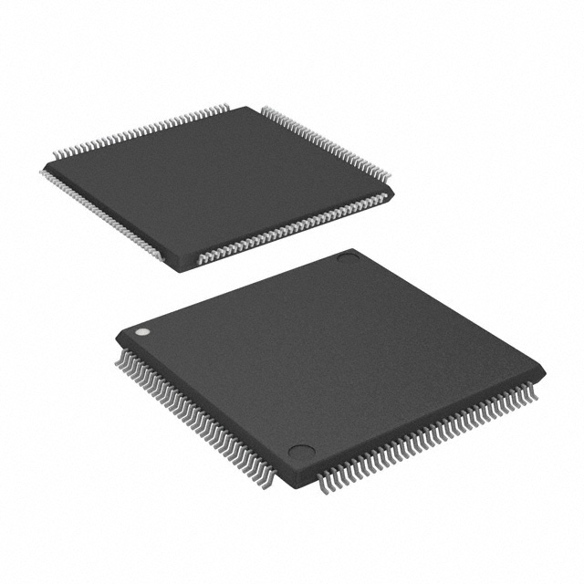
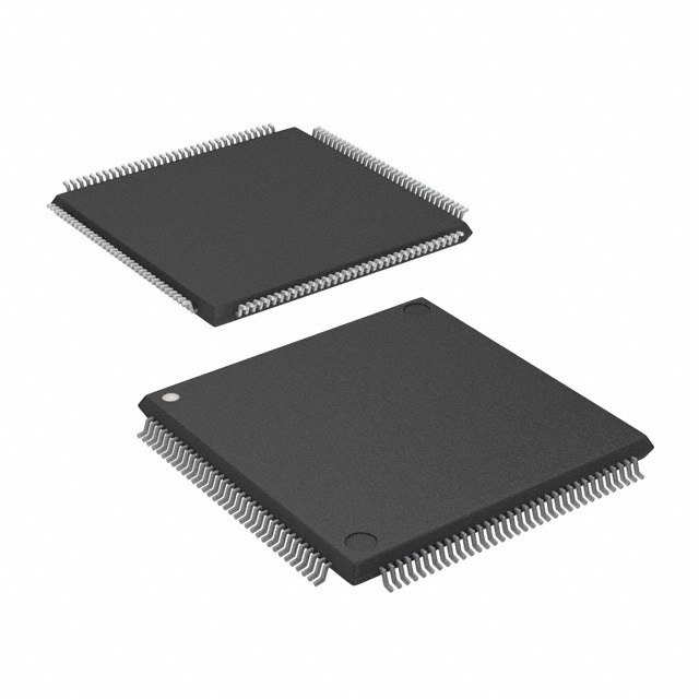
MIPS-II Microprocessor IC Interprise™ 1 Core, 32-Bit 150MHz 256-PBGA (17x17) |
|---|---|
| Quantity | 1,174 Available (as of October 8, 2026) |

| Product Category | Microprocessors |
|---|---|
| Part Series | IDT79RC32V334 |
| Manufacturer | Renesas Electronics Corporation |
| Manufacturing Status | Obsolete |
| Manufacturer Standard Lead Time | Contact Us |
| Datasheet |
Specifications & Environmental
| Core Processor | MIPS-II | Device Package | 256-PBGA (17x17) | Mounting Type | Surface Mount | ||
|---|---|---|---|---|---|---|---|
| Number of Cores/Bus Width | 1 Core, 32-Bit | Operating Temperature | 0°C – 70°C | Package / Case | Tray | ||
| Speed | 150MHz | Voltage | 3.3V |
Overview of IDT79RC32V334-150BB – MIPS‑II 32‑Bit MPU, 150 MHz, 256‑PBGA
The IDT79RC32V334-150BB is a single‑core, 32‑bit microprocessor based on the MIPS‑II instruction set, specified for operation up to 150 MHz. Designed for embedded and consumer applications, it integrates CPU, memory controllers and a wide set of peripherals to simplify system design and reduce external components.
With on‑chip caches, an MMU and comprehensive I/O support, this device targets embedded communications and general‑purpose embedded designs that require a balanced combination of CPU performance, memory interface flexibility and peripheral integration.
Key Features
- Core: RC32300 MIPS‑II CPU core, single 32‑bit core supporting up to 150 MHz operation and both big and little endian modes.
- Cache & MMU: 8 kB instruction cache (2‑way, lockable) and 2 kB data cache (2‑way, lockable); MMU with a 32‑entry page TLB and cache control options for write‑back/write‑through policies.
- Memory Controllers: Integrated SDRAM controller supporting 4 non‑interleaved banks and up to 512 MB total SDRAM; memory & peripheral controller with 6 banks supporting 8‑, 16‑ and 32‑bit interfaces for Flash, SRAM and other devices.
- DMA: Four general‑purpose DMA channels with support for scatter/gather, chaining, endian swapping and unaligned transfers; programmable burst sizes up to 16 bytes.
- Bus & PCI: Local bus interface (up to 75 MHz, 26‑bit address, 32‑bit data) and 32‑bit PCI interface (up to 66 MHz, PCI rev. 2.2 compatible) supporting target and master roles.
- Peripherals & Serial Interfaces: Two 16550‑compatible UARTs (baud support to 1.5 Mb/s), SPI master, programmable I/O (PIO) and four 32‑bit timer/counters for system control and serial communications.
- System & Debug: Interrupt controller, EJTAG in‑circuit emulator interface and IEEE‑1149.1 JTAG support for debug and test.
- Package & Power: 256‑ball PBGA (17 × 17 mm, 1.0 mm ball spacing), surface mount; 3.3 V operation with 5 V tolerant I/O.
- Environmental & Qualification: Consumer qualification and RoHS compliant; operating temperature range 0 °C to 70 °C.
Typical Applications
- Embedded Communications: Integration of CPU, DMA, PCI and serial interfaces makes this device suitable for embedded communications controllers and networking endpoints.
- Consumer Embedded Devices: Consumer‑grade embedded systems that require a single 32‑bit core, on‑chip memory controllers and UART/SPI connectivity.
- Board‑Level System Control: Local bus and peripheral controller features enable direct control of memory and onboard peripherals for compact system designs.
Unique Advantages
- Integrated Memory Subsystem: On‑chip SDRAM controller and multi‑bank memory/peripheral controller reduce external memory interface complexity and BOM.
- Flexible DMA and Bus Options: Four DMA channels with scatter/gather and PCI/local bus support streamline high‑throughput data movement without CPU intervention.
- Deterministic Cache Control: Lockable instruction and data caches plus programmable cache algorithms provide control over memory behavior for latency‑sensitive embedded tasks.
- Comprehensive Peripheral Set: UARTs, SPI, timers, PIO and PCI connectivity provide versatile I/O options for varied embedded system requirements.
- Debug and Development Support: EJTAG and JTAG interfaces along with documented processor features support hardware debug and development workflows.
- Compact, Industry‑Standard Package: 256‑ball PBGA (17×17 mm) enables a compact board footprint with surface‑mount assembly.
Why Choose IDT79RC32V334-150BB?
The IDT79RC32V334-150BB positions itself as a balanced, integrated solution for embedded and consumer designs that need a MIPS‑II 32‑bit core running up to 150 MHz combined with on‑chip memory controllers, DMA, PCI and serial peripherals. Its mix of cache, MMU and configurable memory interfaces offers designers control over performance and memory behavior without adding excessive external logic.
This device is suitable for teams building embedded communications controllers, consumer embedded products and board‑level controllers where integration, interface flexibility and available debug support help shorten development time and simplify system architecture.
Request a quote or submit an inquiry to receive pricing and availability for the IDT79RC32V334-150BB and to discuss how it fits your next embedded design.




















Date Founded: 2002
Headquarters: Koto City, Tokyo, Japan
Employees: 21,000+
Revenue: $10 Billion
Certifications and Memberships: ISO9001:2015, IATF16949:2016


