
LS1048ASN7Q1A
| Part Description |
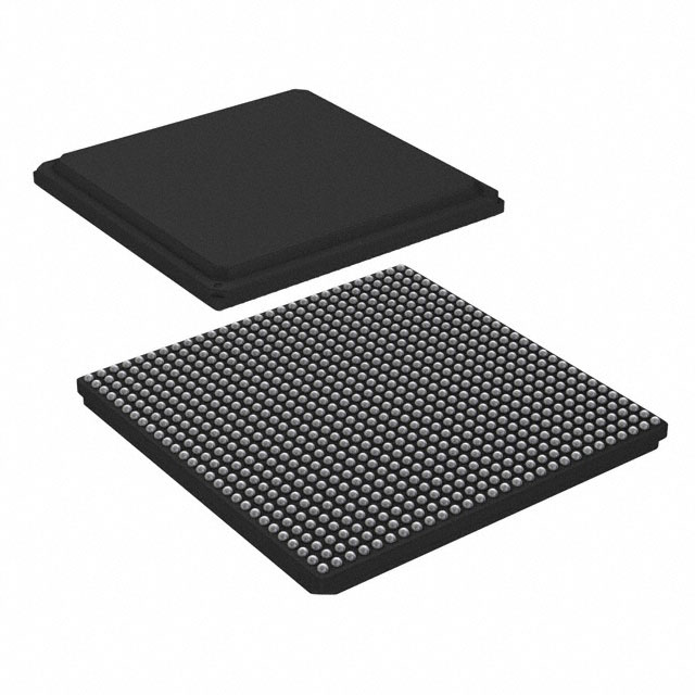
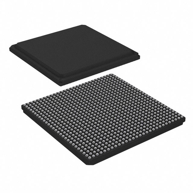
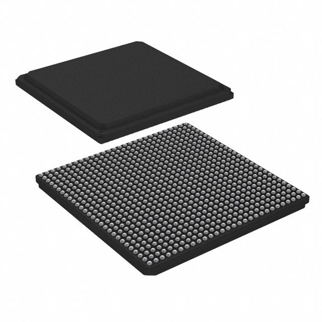
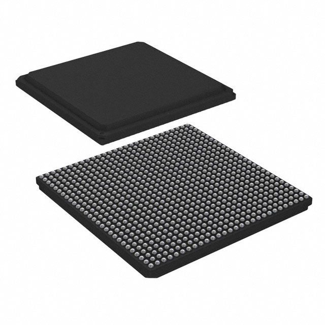
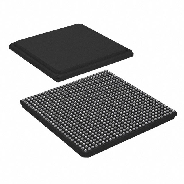
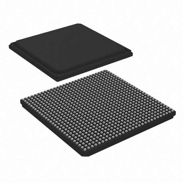
ARM® Cortex®-A53 Microprocessor IC QorIQ® Layerscape 4 Core, 64-Bit 1.6GHz 780-FBGA (23x23) |
|---|---|
| Quantity | 120 Available (as of October 8, 2026) |
| Product Category | Microprocessors |
|---|---|
| Part Series | LS1048A |
| Manufacturer | NXP USA Inc. |
| Manufacturing Status | Active |
| Manufacturer Standard Lead Time | 18 Weeks |
| Datasheet |
Specifications & Environmental
| Core Processor | ARM® Cortex®-A53 | Device Package | 780-FBGA (23x23) | ECCN | 5A002A1 FRE | ||
|---|---|---|---|---|---|---|---|
| Ethernet | 10GbE (2), 1GbE (8) | HTS Code | 8542.31.0001 | Moisture Sensitivity Level | 3 (168 Hours) | ||
| Mounting Method | Surface Mount | Mounting Type | Surface Mount | Number of Cores/Bus Width | 4 Core, 64-Bit | ||
| Operating Temperature | 0°C ~ 105°C | Package / Case | 780-BFBGA, FCBGA | RAM Controllers | DDR4 | ||
| REACH Compliance | REACH Unaffected | RoHS Compliance | ROHS3 Compliant | SATA | SATA 6Gbps (1) | ||
| Security Features | Secure Boot, TrustZone® | Speed | 1.6GHz | Supplier Device Package | 780-FBGA (23×23) | ||
| USB | USB 3.0 (2) + PHY |
Overview of LS1048ASN7Q1A – IC MPU QORIQ 1.6GHZ 780FBGA
The LS1048ASN7Q1A is an NXP QorIQ Layerscape microprocessor featuring four ARM® Cortex®-A53 64-bit cores running at 1.6 GHz in a 780‑FBGA (23 × 23 mm) package. Designed for embedded and communications applications, the device integrates high-performance processing, multi-gigabit networking interfaces and memory controllers to support intelligent edge and networking use cases.
Built around NXP’s datapath acceleration architecture (DPAA2) and supported by an NXP software development toolkit, the LS1048ASN7Q1A targets intelligent edge access, virtual CPE/NFV solutions, wireless access point control and industrial designs that require integrated networking, security and peripheral connectivity.
Key Features
- Core and Architecture Four ARM® Cortex®-A53 64-bit cores at 1.6 GHz providing multicore general-purpose processing.
- Memory DDR4 memory controller support for modern system memory performance and capacity.
- Networking Integrated multi-gigabit Ethernet interfaces: 2 × 10GbE and 8 × 1GbE to support high-density networking and connectivity scenarios.
- Storage and USB SATA 6 Gbps (1) for direct storage attachment and 2 × USB 3.0 ports with PHY for high-speed peripheral connectivity.
- Security Secure Boot and TrustZone® hardware security features for platform integrity and trusted execution.
- Package and Mounting 780‑FBGA (23 × 23 mm) FCBGA package, surface mount, suitable for compact embedded system designs.
- Operating Range and Qualification Operating temperature 0 °C to 105 °C and consumer qualification; RoHS compliant.
- Datapath Acceleration and Software Includes NXP’s DPAA2 datapath acceleration architecture and is supported by NXP software toolkit resources for accelerated network and I/O handling.
Typical Applications
- Intelligent Edge Access Acts as a compute and network offload engine for edge devices that require integrated networking and security.
- Network Functions Virtualization (NFV) / vCPE Enables virtualized customer-premises equipment and NFV solutions with multicore processing and DPAA2 acceleration.
- Wireless Access Point Control Provides control-plane processing and multiple Ethernet interfaces for wireless access point and gateway designs.
- Industrial Networking Serves industrial communication and control use cases that benefit from multiport Ethernet, hardware security and DDR4 memory support.
Unique Advantages
- High-performance multicore processing: Four ARM® Cortex®-A53 64-bit cores at 1.6 GHz deliver balanced compute for control-plane and data-plane tasks.
- Integrated high-density networking: Multiple 10GbE and 1GbE interfaces simplify designs that require aggregated or segmented network connectivity.
- Built-in security features: Secure Boot and TrustZone® support platform integrity and enable trusted software execution models.
- Datapath acceleration (DPAA2): Hardware datapath acceleration architecture and associated accelerators reduce CPU load for network and I/O processing.
- Flexible storage and peripheral I/O: SATA 6 Gbps plus USB 3.0 with PHY provide direct attachment options for storage and high-speed peripherals.
- Compact, production-ready package: 780‑FBGA (23 × 23 mm) surface-mount package and consumer qualification with RoHS compliance support rapid integration into embedded products.
Why Choose LS1048ASN7Q1A?
The LS1048ASN7Q1A positions itself as a balanced, integrated application processor for embedded networking and intelligent edge systems. With four ARM® Cortex®-A53 cores, DDR4 memory support, extensive Ethernet connectivity and DPAA2 acceleration, it combines the processing, I/O and security capabilities needed for modern edge and communications designs.
This device is well suited to designers building virtual CPE, NFV, access point controllers and industrial networking equipment who require a compact, RoHS‑compliant processor offering integrated networking ports, storage and hardware security, plus software support from NXP’s development toolkit.
Request a quote or submit a procurement inquiry to begin an evaluation and obtain pricing and availability information for LS1048ASN7Q1A.



















Date Founded: 2006
Headquarters: Eindhoven, North Brabant, Netherlands
Employees: 38,000+
Revenue: $10.53 Billion
Certifications and Memberships: ISO9001:2015, IATF16949:2016


