
LS2044ASE711B
| Part Description |
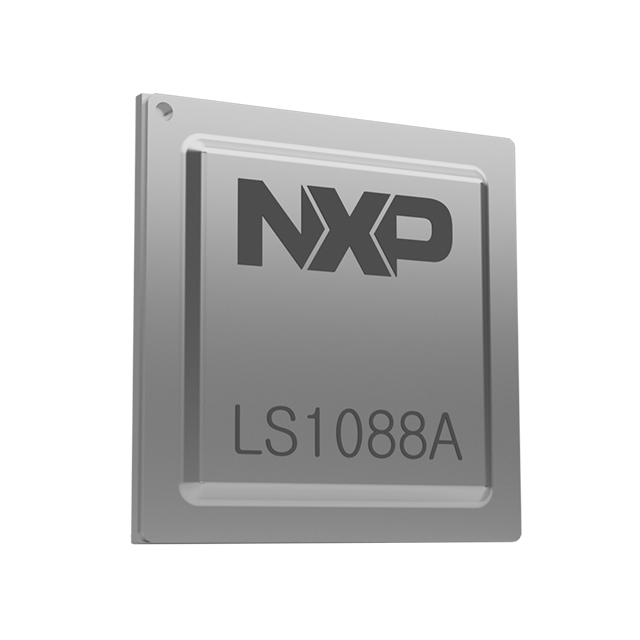
ARM® Cortex®-A72 Microprocessor IC QorIQ® Layerscape 4 Core, 64-Bit 2.1GHz 1292-FCPBGA (37.5x37.5) |
|---|---|
| Quantity | 688 Available (as of October 8, 2026) |

| Product Category | Microprocessors |
|---|---|
| Part Series | LS2044A |
| Manufacturer | NXP USA Inc. |
| Manufacturing Status | Active |
| Manufacturer Standard Lead Time | 18 Weeks |
| Datasheet |
Specifications & Environmental
| Core Processor | ARM® Cortex®-A72 | Device Package | 1292-FCPBGA (37.5x37.5) | ECCN | N/A | ||
|---|---|---|---|---|---|---|---|
| Ethernet | 10GbE (8), 1GbE (16), 2.5GbE (1) | Graphics Acceleration | No | HTS Code | N/A | ||
| Moisture Sensitivity Level | 3 (168 Hours) | Mounting Method | Surface Mount | Mounting Type | Surface Mount | ||
| Number of Cores/Bus Width | 4 Core, 64-Bit | Operating Temperature | 0°C ~ 105°C (TA) | Package / Case | 1292-BBGA, FCBGA | ||
| RAM Controllers | DDR4 | REACH Compliance | REACH Unaffected | RoHS Compliance | ROHS3 Compliant | ||
| SATA | SATA 6Gbps (2) | Security Features | Secure Boot, TrustZone® | Speed | 2.1GHz | ||
| Supplier Device Package | 1292-FCPBGA (37.5×37.5) | USB | USB 3.0 + PHY (2) |
Overview of LS2044ASE711B – IC MPU QORIQ 2.1GHZ 1292FCPBGA
The LS2044ASE711B is an NXP QorIQ Layerscape microprocessor IC based on 64‑bit ARM® Cortex®‑A72 cores. This 4‑core device runs up to 2.1 GHz and integrates a high‑bandwidth memory subsystem, datapath acceleration, and extensive high‑speed I/O in a 1292‑ball FCPBGA package.
Engineered for embedded networking, security and storage-focused designs, the LS2044ASE711B delivers a combination of compute performance, datapath offload and system integration to help reduce board-level complexity and accelerate time to market.
Key Features
- Processor Core ARM® Cortex®‑A72 architecture, 4 cores, 64‑bit operation at up to 2.1 GHz.
- Memory Subsystem Two 64‑bit DDR4 SDRAM controllers with ECC and interleaving support plus a 1 MB platform cache with ECC protection.
- Datapath Acceleration (DPAA2) Integrated DPAA2 with Wire‑rate IO Processor (WRIOP) for packet parsing/classification, queue management (QBMan), hardware buffer management, and accelerators for cryptography (SEC 5.2), RegEx pattern matching (PME 2.0) and compression/decompression (DCE 1.0).
- High‑Speed Networking Up to eight 10 Gbps Ethernet MACs and up to sixteen 1/2.5 Gbps Ethernet MACs (specification lists 10GbE (8), 1GbE (16), 2.5GbE (1)).
- Peripheral Interfaces Two SATA 6 Gbps controllers, two USB 3.0 controllers with integrated PHY, four PCIe 3.0 controllers with flexible lane widths, 16 SerDes lanes (up to 10.3125 GHz), and multiple I2C controllers.
- Security & System Management Secure Boot and TrustZone® support plus a service processor for pre‑boot initialization and secure‑boot capabilities; hardware support for virtualization and partitioning enforcement.
- System Integration & DMA qDMA engine, hardware queue and buffer management to streamline packet and data movement.
- Package & Environmental 1292‑FCPBGA (37.5 × 37.5 mm) surface‑mount package, RoHS compliant, operating temperature range 0 °C to 105 °C.
Typical Applications
- Edge and Enterprise Networking High‑throughput packet handling using multiple 10GbE/1GbE MACs combined with DPAA2 acceleration for packet parsing and classification.
- Network Security Appliances Offload cryptographic workloads with SEC 5.2 acceleration and use TrustZone® and Secure Boot for trusted system operation.
- Storage and NAS Systems Integrate high‑bandwidth storage via dual SATA 6 Gbps controllers and PCIe 3.0 connectivity for host and expansion interfaces.
- Virtualized and Accelerated Platforms Leverage hardware virtualization features, multiple PCIe controllers and high memory bandwidth for partitioned or virtualized service deployments.
Unique Advantages
- High compute density: Four ARM® Cortex®‑A72 cores at up to 2.1 GHz provide substantial application-level performance for embedded servers and edge compute.
- Datapath offload: DPAA2 accelerators (packet parsing, queue management, cryptography, PME, DCE) reduce CPU load for networking and security functions.
- Extensive integrated I/O: Multiple 10GbE/1GbE MACs, SATA, USB 3.0, PCIe 3.0 and high‑speed SerDes lanes minimize external bridging and simplify system design.
- Data integrity and memory robustness: Dual 64‑bit DDR4 controllers with ECC and a 1 MB ECC‑protected platform cache support resilient data handling.
- Secure boot and management: Secure Boot, TrustZone® and a service processor provide a secure initialization and runtime foundation.
- Design‑ready packaging: 1292‑FCPBGA surface‑mount package and RoHS compliance ease integration into production hardware.
Why Choose LS2044ASE711B?
The LS2044ASE711B positions itself as a performance‑oriented Layerscape solution that balances multi‑core ARM® processing with dedicated datapath acceleration and broad I/O integration. Its combination of Cortex‑A72 cores, DPAA2 acceleration, ECC‑protected memory and multiple high‑speed interfaces makes it suitable for developers building networking, security, storage and virtualized edge solutions that require integrated offload and throughput.
For system designers and procurement teams looking for a consumer‑qualified embedded MPU that simplifies board‑level architecture while providing secure boot, cryptographic acceleration and flexible connectivity, the LS2044ASE711B offers a compact, RoHS‑compliant platform in a 1292‑ball FCPBGA package.
Request a quote or submit an inquiry to learn about pricing and availability for the LS2044ASE711B and to discuss how it fits your next embedded networking or storage design.


















Date Founded: 2006
Headquarters: Eindhoven, North Brabant, Netherlands
Employees: 38,000+
Revenue: $10.53 Billion
Certifications and Memberships: ISO9001:2015, IATF16949:2016


