
5AGXBB1D4F40C4G
| Part Description |
Arria V GX Field Programmable Gate Array (FPGA) IC 704 17358848 300000 1517-BBGA, FCBGA |
|---|---|
| Quantity | 1,758 Available (as of June 15, 2026) |
| Product Category | Field Programmable Gate Array (FPGA) |
|---|---|
| Manufacturer | Intel |
| Manufacturing Status | Active |
| Manufacturer Standard Lead Time | 12 Weeks |
| Datasheet |
Specifications & Environmental
| Device Package | 1517-FBGA, FC (40x40) | Grade | Commercial | Operating Temperature | 0°C – 85°C | ||
|---|---|---|---|---|---|---|---|
| Package / Case | 1517-BBGA, FCBGA | Number of I/O | 704 | Voltage | 1.07 V - 1.13 V | ||
| Mounting Method | Surface Mount | RoHS Compliance | RoHS Compliant | REACH Compliance | REACH Unaffected | ||
| Moisture Sensitivity Level | 3 (168 Hours) | Number of LABs/CLBs | 14151 | Number of Logic Elements/Cells | 300000 | ||
| Number of Gates | N/A | ECCN | PENDING ECCN | HTS Code | 0000.00.0000 | ||
| Qualification | N/A | Total RAM Bits | 17358848 |
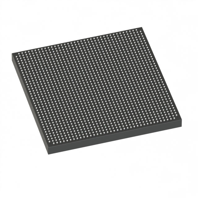
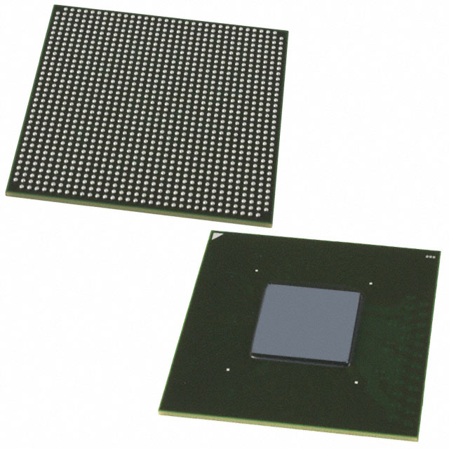
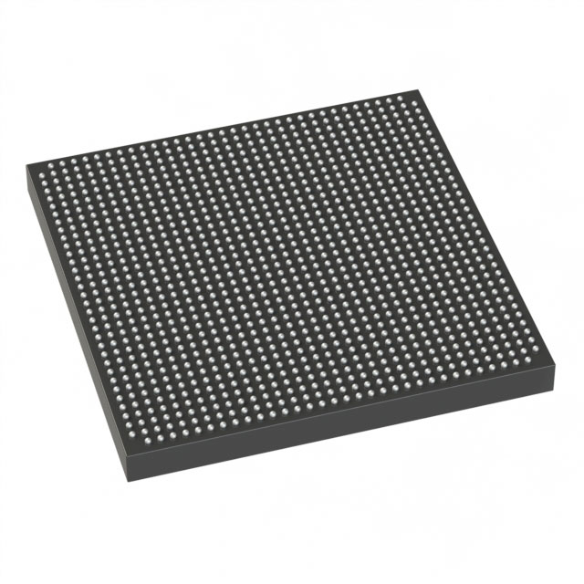
Overview of 5AGXBB1D4F40C4G – Arria V GX FPGA, 300,000 logic elements, 704 I/O, 1517-BBGA
The 5AGXBB1D4F40C4G is an Intel Arria V GX field-programmable gate array (FPGA) offered in a 1517-BBGA FCBGA package. With 300,000 logic elements and approximately 17.36 Mbits of embedded RAM, this commercial-grade device delivers high logic density and sizable on-chip memory for complex, programmable designs. Its 704 general-purpose I/O pins and single-core voltage range of 1.07 V to 1.13 V provide the electrical foundation for dense I/O and logic-centric systems.
The device is RoHS compliant and specified for commercial operating temperatures from 0 °C to 85 °C, making it suitable for a wide range of standard electronic applications where high logic capacity and extensive I/O are required.
Key Features
- High Logic Density — 300,000 logic elements to implement complex logic, control, and data-processing functions on-chip.
- On‑Chip Memory — Total embedded RAM of 17,358,848 bits (approximately 17.36 Mbits) to support buffering, lookup tables, and local data storage.
- Extensive I/O — 704 I/O pins to connect to multiple peripherals, interfaces, and high-channel-count front-ends.
- Package and Mounting — 1517-BBGA, FCBGA package with supplier package listed as 1517-FBGA, FC (40×40); surface-mount design simplifies board assembly.
- Power and Operating Range — Core supply specified between 1.07 V and 1.13 V; commercial-grade operating temperature from 0 °C to 85 °C.
- Design and Configuration Documentation — Comprehensive device datasheet coverage includes electrical characteristics, switching characteristics, core and transceiver performance, I/O timing, and configuration specifications such as POR, JTAG, Fast Passive Parallel (FPP), Active Serial (AS), and Passive Serial (PS).
- Regulatory — RoHS compliant for materials and process compliance.
Typical Applications
- High-density logic systems: Implement large custom logic blocks and state machines using the device’s 300,000 logic elements and abundant embedded RAM.
- Multi-channel I/O aggregation: Systems that require hundreds of I/Os for sensor arrays, parallel interfaces, or expansion daughtercards can leverage the 704 available I/O pins.
- On-board buffering and local memory: Applications needing significant on-chip RAM for FIFOs, packet buffering, or LUT-based processing benefit from approximately 17.36 Mbits of embedded RAM.
- Product development and prototyping: Commercial-grade designs targeting standard temperature ranges and RoHS compliance can use this Arria V GX device for system validation and pre-production runs.
Unique Advantages
- Substantial logic resources: 300,000 logic elements enable consolidation of multiple functions into a single FPGA, reducing component count and board complexity.
- Large embedded RAM footprint: Approximately 17.36 Mbits of on-chip memory supports local buffering and data-centric algorithms without immediate external memory dependence.
- High I/O count: 704 I/O pins provide flexibility for dense interfacing, minimizing the need for external multiplexing or expanders.
- Surface-mount BBGA package: The 1517-BBGA/1517-FBGA (40×40) footprint supports compact, automated assembly and consistent thermal/electrical characteristics.
- Comprehensive configuration support: The datasheet documents multiple configuration schemes and timing specifications (POR, JTAG, FPP, AS, PS), aiding hardware bring-up and system integration.
- RoHS compliant: Material compliance supports regulatory requirements for lead-free assemblies.
Why Choose 5AGXBB1D4F40C4G?
The 5AGXBB1D4F40C4G Arria V GX FPGA is positioned for designs that require a high concentration of programmable logic, abundant on-chip memory, and a large number of I/Os in a compact surface-mount package. Its documented electrical, switching, and configuration specifications help streamline integration and verification for commercial-temperature applications.
Choose this device when your design prioritizes logic density, on-chip RAM capacity, and I/O flexibility while maintaining RoHS compliance and standard commercial-grade operating conditions.
Request a quote or submit a product inquiry to evaluate the 5AGXBB1D4F40C4G for your next design project.


Date Founded: 1968
Headquarters: Santa Clara, California, USA
Employees: 130,000+
Revenue: $54.23 Billion
Certifications and Memberships: ISO9001:2015, ISO14001:2015, ISO17025:2017, ISO27001:2022, ISO45001:2018, ISO50001:2018


