
A3PN060-Z2VQ100I
| Part Description |
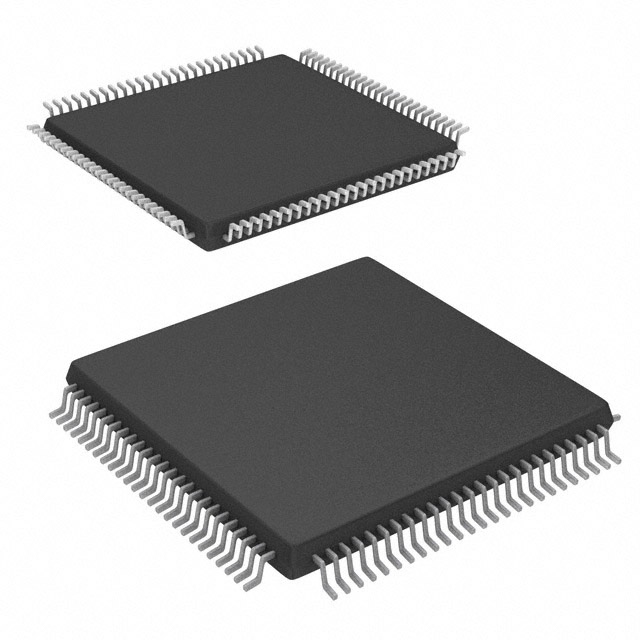
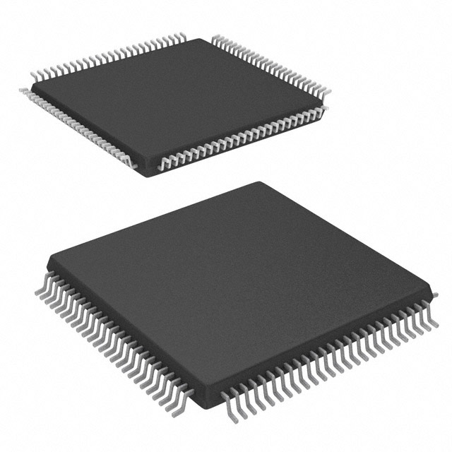
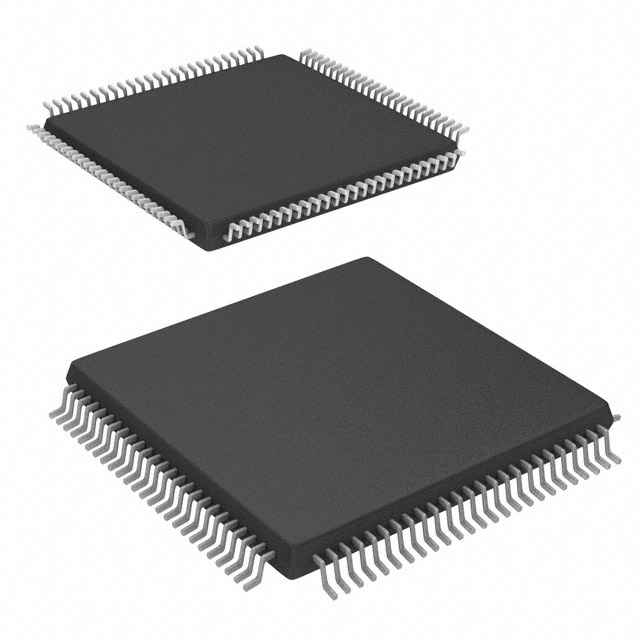
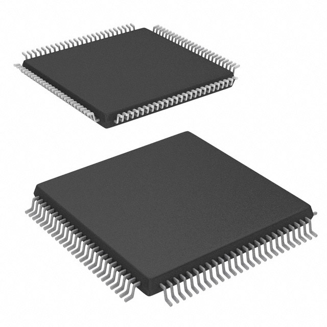
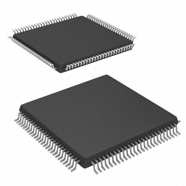
ProASIC3 nano Field Programmable Gate Array (FPGA) IC 71 18432 100-TQFP |
|---|---|
| Quantity | 690 Available (as of October 7, 2026) |
| Product Category | Field Programmable Gate Array (FPGA) |
|---|---|
| Manufacturer | Microchip Technology |
| Manufacturing Status | Obsolete |
| Manufacturer Standard Lead Time | Contact Us |
| Datasheet |
Specifications & Environmental
| Device Package | 100-VQFP (14x14) | Grade | Industrial | Operating Temperature | -40°C – 100°C | ||
|---|---|---|---|---|---|---|---|
| Package / Case | 100-TQFP | Number of I/O | 71 | Voltage | 1.425 V - 1.575 V | ||
| Mounting Method | Surface Mount | RoHS Compliance | RoHS non-compliant | REACH Compliance | REACH Unaffected | ||
| Moisture Sensitivity Level | 3 (168 Hours) | Number of LABs/CLBs | 1536 | Number of Logic Elements/Cells | 1536 | ||
| Number of Gates | 60000 | ECCN | 3A991D | HTS Code | 8542.39.0001 | ||
| Qualification | N/A | Total RAM Bits | 18432 |
Overview of A3PN060-Z2VQ100I – ProASIC3 nano Field Programmable Gate Array (FPGA) IC 71 18432 100-TQFP
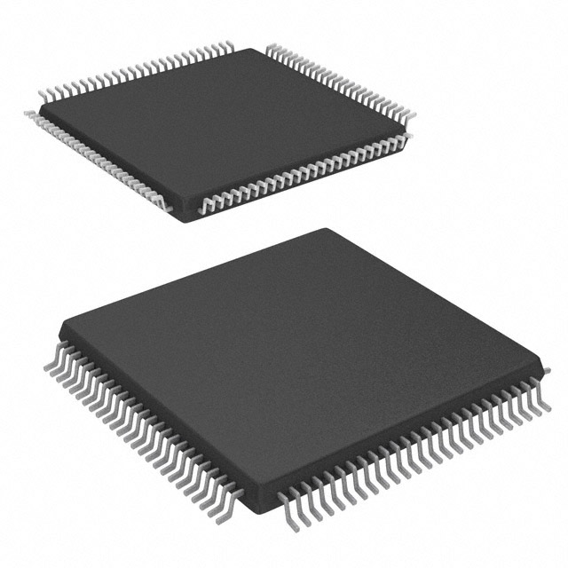
The A3PN060-Z2VQ100I is a ProASIC3 nano flash-based FPGA from Microchip Technology. It implements the ProASIC3 nano FPGA fabric and provides a compact, surface-mount logic platform with embedded memory, programmable logic, and 71 general I/Os.
Designed for industrial-grade applications, the device combines 1,536 logic elements, approximately 18,432 bits of embedded RAM, and about 60,000 gates in a 100-pin TQFP package. The device supports low-power operating modes and is specified over a wide industrial temperature range.
Key Features
- Core Logic — 1,536 logic elements (cells) delivering flexible programmable logic resources and approximately 60,000 gates for custom logic implementations.
- Embedded Memory — Approximately 18,432 bits of on-chip RAM to support buffering, state machines, and small memory structures without external RAM.
- I/O Density — 71 I/Os to support peripheral interfacing, I/O aggregation, and board-level glue logic in a single device.
- Low-Power Modes — The ProASIC3 nano fabric supports multiple low-power states documented in the user guide, including Static (Idle), User Low Static, Sleep, and Shutdown modes for power-sensitive designs.
- Global Resources & Clocking — Device architecture documentation references global resource distribution, VersaNet global network distribution, spine architecture, and clock aggregation features for scalable routing and clock management.
- Package & Mounting — Surface-mount 100-TQFP package (supplier device package listed as 100-VQFP 14×14) for compact PCB integration.
- Power Supply — Specified core voltage range from 1.425 V to 1.575 V for supply planning and power budgeting.
- Industrial Temperature Grade — Specified operating range from −40 °C to 100 °C for deployment in industrial environments.
- Regulatory Status — RoHS compliant.
Typical Applications
- Industrial Control — Use the device’s industrial temperature range and programmable logic for control, sequencing, and I/O aggregation in industrial equipment.
- Embedded Logic Integration — Implement board-level glue logic, custom peripherals, and protocol translation using available logic elements and 71 I/Os.
- Low-Power Systems — Leverage multiple documented low-power modes for designs where minimizing standby and idle power is required.
Unique Advantages
- Compact, Surface-Mount Integration: 100-pin TQFP packaging and surface-mount mounting simplify PCB layout while providing a substantial I/O count for its footprint.
- Flash-Based FPGA Fabric: ProASIC3 nano fabric provides programmable logic and on-chip RAM without the need for external configuration memory.
- Documented Low-Power Strategies: Multiple low-power operating modes are described in the device documentation, enabling designers to optimize power for idle and active states.
- Industrial Temperature Support: Specified −40 °C to 100 °C operation supports deployment in demanding environments where temperature resilience is required.
- Balanced Logic and Memory: 1,536 logic elements combined with approximately 18,432 bits of embedded RAM enable a range of control and data-path functions on-chip.
Why Choose A3PN060-Z2VQ100I?
The A3PN060-Z2VQ100I positions itself as a compact, industrial-grade flash FPGA that brings together a practical mix of programmable logic, embedded RAM, and I/O density in a 100-pin surface-mount package. Its documented low-power modes and architecture-level resources make it suitable for designs that require on-chip flexibility with controlled power consumption.
This device is well suited to engineers and procurement teams seeking a reliable, flash-based FPGA with industrial temperature support, clear power-supply specifications, and a manageable logic/memory balance for embedded control, interface consolidation, and low-power applications.
Request a quote or submit a purchasing inquiry to obtain pricing and availability for the A3PN060-Z2VQ100I.





















Date Founded: 1989
Headquarters: Chandler, Arizona, USA
Employees: 22,000+
Revenue: $8.349 Billion
Certifications and Memberships: ISO9001:2015, IATF16949:2016, AS 9100D




