
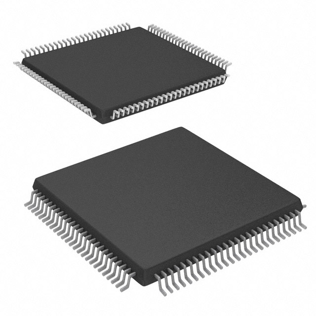
A3PN250-ZVQ100
| Part Description |
ProASIC3 nano Field Programmable Gate Array (FPGA) IC 68 36864 100-TQFP |
|---|---|
| Quantity | 222 Available (as of June 15, 2026) |

| Product Category | Field Programmable Gate Array (FPGA) |
|---|---|
| Manufacturer | Microchip Technology |
| Manufacturing Status | Obsolete |
| Manufacturer Standard Lead Time | Contact Us |
| Datasheet |
Specifications & Environmental
| Device Package | 100-VQFP (14x14) | Grade | Commercial | Operating Temperature | -20°C – 85°C | ||
|---|---|---|---|---|---|---|---|
| Package / Case | 100-TQFP | Number of I/O | 68 | Voltage | 1.425 V - 1.575 V | ||
| Mounting Method | Surface Mount | RoHS Compliance | RoHS non-compliant | REACH Compliance | REACH Unaffected | ||
| Moisture Sensitivity Level | 3 (168 Hours) | Number of LABs/CLBs | 6144 | Number of Logic Elements/Cells | 6144 | ||
| Number of Gates | 250000 | ECCN | 3A991D | HTS Code | 8542.39.0001 | ||
| Qualification | N/A | Total RAM Bits | 36864 |
Overview of A3PN250-ZVQ100 – ProASIC3 nano Field Programmable Gate Array (FPGA) IC 68 36864 100-TQFP
The A3PN250-ZVQ100 is a ProASIC3 nano flash-based FPGA from Microchip Technology. It provides a compact, low-power programmable logic fabric with 6,144 logic elements, on-chip embedded memory, and 68 general-purpose I/Os in a 100-pin TQFP package.
Designed for commercial-grade embedded designs, the device combines a flash-configured FPGA fabric with multiple low-power modes and global resource support to address applications that require small form factor programmable logic, deterministic configuration and low static power.
Key Features
- Logic Capacity Approximately 6,144 logic elements (6144 logic elements) suitable for compact programmable-logic implementations.
- Embedded Memory Total on-chip RAM: 36,864 bits (approx. 36.9 kbits) of embedded memory for state, buffering and small data structures.
- I/O 68 general-purpose I/Os enabling multiple peripheral and bus connections directly to the FPGA fabric.
- Gate Density Equivalent to 250,000 gates of logic capacity for combining glue logic and small-scale acceleration functions.
- Low-Power Flash Architecture Flash-based configuration with documented low-power operation modes including Static (Idle), User Low Static, Sleep and Shutdown to help manage static and dynamic power.
- Global Resources & Clocking Architecture-level features described in the device family documentation include global resource distribution, VersaNet global network distribution, spine architecture and clock aggregation support for system-level routing and clocking strategies.
- Voltage & Power Single-core supply range specified at 1.425 V to 1.575 V for the FPGA core.
- Package & Mounting 100-TQFP (100-VQFP, 14×14) surface-mount package for compact PCB designs.
- Operating Range Commercial grade with an operating temperature range of −20 °C to 85 °C.
- Compliance RoHS compliant.
Typical Applications
- Embedded Control Logic Use the programmable fabric and on-chip RAM to implement custom control, sequencing and glue logic functions in compact embedded systems.
- Interface Consolidation Leverage 68 I/Os and the device’s global routing resources to consolidate multiple peripheral interfaces into a single programmable device.
- Low-Power Designs Employ the device’s low-power modes and flash-based configuration for battery-aware or always-on applications that benefit from reduced static power.
Unique Advantages
- Flash-Based Nonvolatile Configuration: Flash configuration enables immediate, nonvolatile FPGA behavior at power-up without external configuration memory.
- Small, PCB-Friendly Package: 100-TQFP surface-mount package allows integration into space-constrained PCBs while providing a full complement of I/Os.
- Explicit Low-Power Modes: Documented Static, User Low Static, Sleep and Shutdown modes give designers defined options to reduce power consumption during idle or low-activity periods.
- Balanced Logic and Memory: Combination of ~6,144 logic elements and ~36.9 kbits of on-chip RAM supports control-oriented and buffering tasks without external memory for many applications.
- System-Level Routing Features: Global resource distribution, VersaNet and clock aggregation capabilities described in the device documentation help with deterministic routing and clocking in multi-domain designs.
- Commercial-Grade Temperature Range: Specified −20 °C to 85 °C operating range for general-purpose commercial applications.
Why Choose A3PN250-ZVQ100?
The A3PN250-ZVQ100 is positioned for designers who need a compact, flash-configured FPGA with clearly defined low-power modes, a moderate logic and memory footprint, and a high I/O count in a 100-pin TQFP package. Its combination of ~6,144 logic elements, 36,864 bits of embedded RAM, and architecture-level global routing features make it suitable for embedded control, interface consolidation and other space-constrained programmable logic tasks in commercial products.
Choosing this device provides a balance of integration, predictable nonvolatile configuration and power management options, backed by Microchip Technology’s ProASIC3 nano FPGA documentation and family resources for system-level integration and clocking strategies.
Request a quote or submit a product inquiry to evaluate the A3PN250-ZVQ100 for your next design. Our team can provide pricing, availability and support information to help you move from prototype to production.


Date Founded: 1989
Headquarters: Chandler, Arizona, USA
Employees: 22,000+
Revenue: $8.349 Billion
Certifications and Memberships: ISO9001:2015, IATF16949:2016, AS 9100D


