
A3PN250-Z2VQG100
| Part Description |
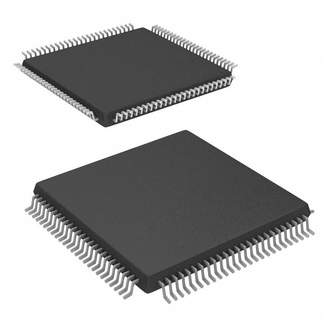
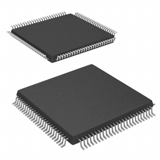
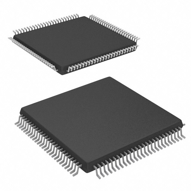
ProASIC3 nano Field Programmable Gate Array (FPGA) IC 68 36864 100-TQFP |
|---|---|
| Quantity | 796 Available (as of October 8, 2026) |
| Product Category | Field Programmable Gate Array (FPGA) |
|---|---|
| Manufacturer | Microchip Technology |
| Manufacturing Status | Obsolete |
| Manufacturer Standard Lead Time | Contact Us |
| Datasheet |
Specifications & Environmental
| Device Package | 100-VQFP (14x14) | Grade | Commercial | Operating Temperature | -20°C – 85°C | ||
|---|---|---|---|---|---|---|---|
| Package / Case | 100-TQFP | Number of I/O | 68 | Voltage | 1.425 V - 1.575 V | ||
| Mounting Method | Surface Mount | RoHS Compliance | Unknown | REACH Compliance | REACH Unaffected | ||
| Moisture Sensitivity Level | 3 (168 Hours) | Number of LABs/CLBs | 6144 | Number of Logic Elements/Cells | 6144 | ||
| Number of Gates | 250000 | ECCN | 3A991D | HTS Code | 8542.39.0001 | ||
| Qualification | N/A | Total RAM Bits | 36864 |
Overview of A3PN250-Z2VQG100 – ProASIC3 nano Field Programmable Gate Array, 68 I/O, 100-TQFP
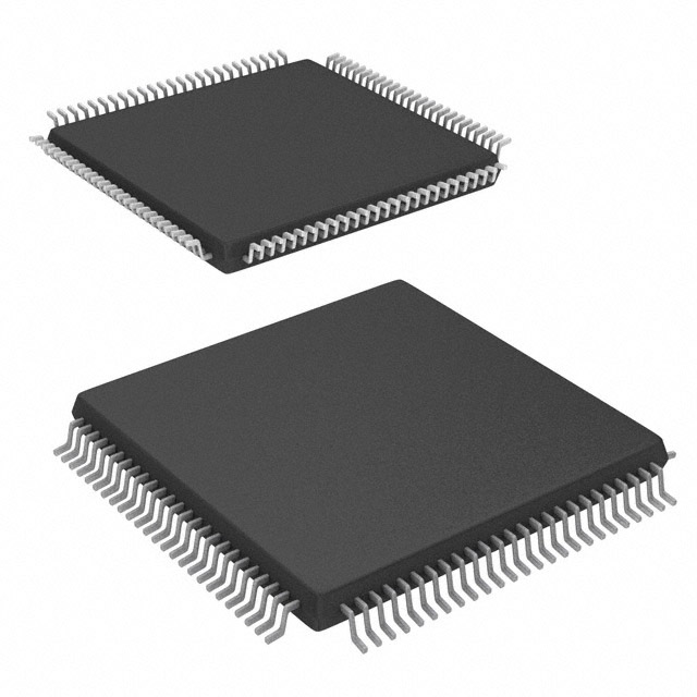
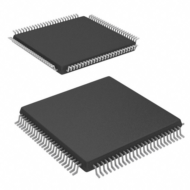
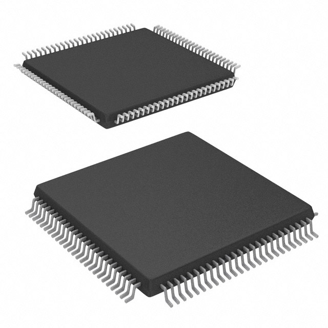
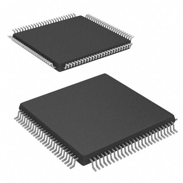
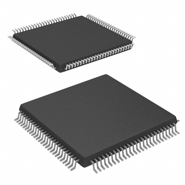
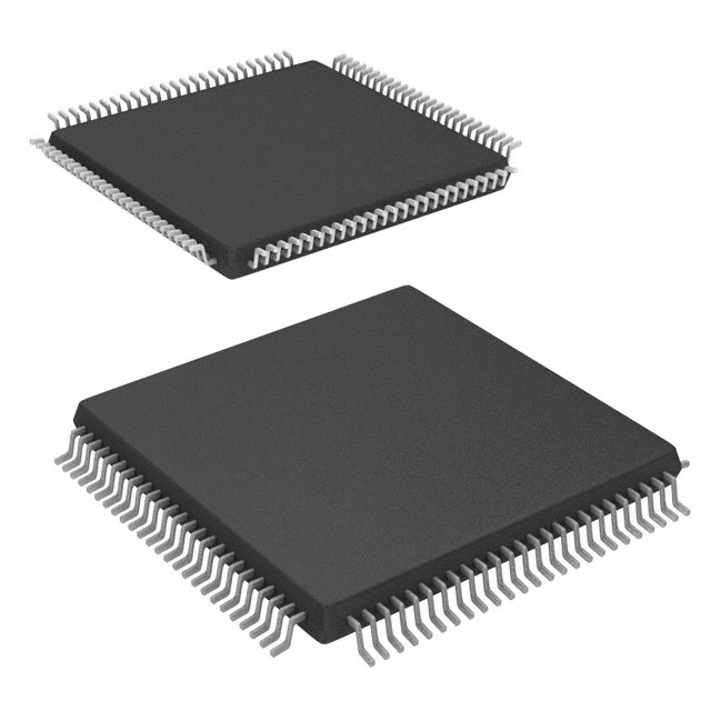
The A3PN250-Z2VQG100 is a ProASIC3 nano family FPGA IC featuring a flash-based, low-power fabric architecture. It provides 6,144 logic elements (LEs), 36,864 bits of on-chip RAM and 68 general-purpose I/Os in a compact 100-pin TQFP (14 × 14 mm) surface-mount package.
Designed for compact, power-conscious embedded designs, the device is targeted at applications that require flexible programmable logic, a moderate logic and memory footprint, and predictable commercial-temperature operation.
Key Features
- Core Logic — 6,144 logic elements and approximately 250,000 equivalent gates provide resources for glue logic, state machines and custom digital functions.
- Embedded Memory — 36,864 total RAM bits of on-chip memory for FIFOs, small buffers and local storage.
- I/O Capacity — 68 general-purpose I/Os to support multiple peripheral interfaces and board-level signal routing.
- Flash-Based, Low-Power Fabric — Series documentation describes low-power modes (Static/Idle, Sleep, Shutdown) and global resource management for energy-conscious designs.
- Power Supply — Core supply voltage specified at 1.425 V to 1.575 V for predictable power domain design.
- Package and Mounting — 100-TQFP (supplier device package 100-VQFP, 14×14 mm) surface-mount package suitable for compact PCB layouts.
- Temperature and Grade — Commercial grade operation from −20 °C to 85 °C.
- Regulatory — RoHS compliant.
Typical Applications
- Embedded Control — Use the 6,144 logic elements and 68 I/Os to implement control logic, state machines and peripheral coordination in compact embedded systems.
- I/O Bridging and Interface Glue — The combination of numerous I/Os and on-chip RAM enables protocol adaptation, bus bridging and timing alignment between subsystems.
- Power-Conscious Designs — Flash-based, low-power architecture and documented low-power modes support designs that require reduced static and dynamic power consumption.
Unique Advantages
- Flash-based FPGA Fabric: The ProASIC3 nano family documentation highlights a flash-based architecture, enabling non-volatile configuration behavior consistent with low-power operation.
- Balanced Integration: 6,144 logic elements, ~36.9kbits of RAM and 68 I/Os provide a balanced set of resources for mid-density logic and interface tasks without excessive board-level components.
- Compact Package: 100-pin TQFP (14 × 14 mm) surface-mount package simplifies PCB routing in space-constrained designs.
- Predictable Power Domain: Defined core supply range (1.425–1.575 V) supports consistent power sequencing and domain planning.
- Commercial Temperature Range: Specified operation from −20 °C to 85 °C for mainstream electronic products and consumer/industrial applications within that range.
- RoHS Compliant: Meets lead-free and hazardous substance requirements for modern manufacturing processes.
Why Choose A3PN250-Z2VQG100?
The A3PN250-Z2VQG100 positions itself as a mid-density, flash-based FPGA solution that combines a practical mix of logic elements, embedded memory and I/O in a compact 100-TQFP package. Its documented low-power modes and flash architecture make it well suited to designs that prioritize power efficiency and reliable configuration behavior.
Choose this device for embedded designs that require programmable logic for interface control, protocol adaptation or moderate computation tasks, while benefiting from a predictable power and thermal envelope and RoHS-compliant manufacturing readiness.
Request a quote or submit an inquiry to receive pricing, lead-time and availability for the A3PN250-Z2VQG100.





















Date Founded: 1989
Headquarters: Chandler, Arizona, USA
Employees: 22,000+
Revenue: $8.349 Billion
Certifications and Memberships: ISO9001:2015, IATF16949:2016, AS 9100D




