
A54SX08A-1TQ100I
| Part Description |
SX-A Field Programmable Gate Array (FPGA) IC 81 100-LQFP |
|---|---|
| Quantity | 1,072 Available (as of June 15, 2026) |

| Product Category | Field Programmable Gate Array (FPGA) |
|---|---|
| Manufacturer | Microchip Technology |
| Manufacturing Status | Obsolete |
| Manufacturer Standard Lead Time | Contact Us |
| Datasheet |
Specifications & Environmental
| Device Package | 100-TQFP (14x14) | Grade | Industrial | Operating Temperature | -40°C – 85°C | ||
|---|---|---|---|---|---|---|---|
| Package / Case | 100-LQFP | Number of I/O | 81 | Voltage | 2.25 V - 5.25 V | ||
| Mounting Method | Surface Mount | RoHS Compliance | RoHS non-compliant | REACH Compliance | REACH Unaffected | ||
| Moisture Sensitivity Level | 3 (168 Hours) | Number of LABs/CLBs | 768 | Number of Logic Elements/Cells | 768 | ||
| Number of Gates | 12000 | ECCN | 3A991D | HTS Code | 8542.39.0001 | ||
| Qualification | N/A |
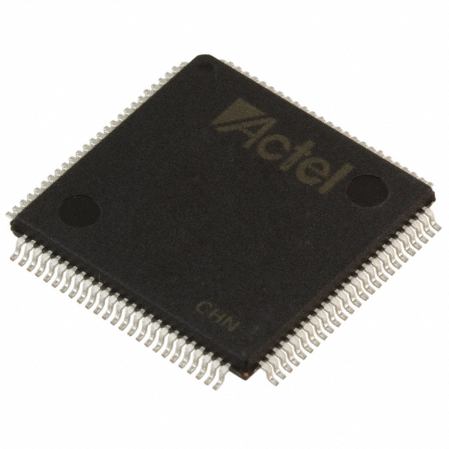
Overview of A54SX08A-1TQ100I – SX-A Field Programmable Gate Array (FPGA) IC, 81 I/O, 100‑LQFP
The A54SX08A-1TQ100I is an SX‑A family field programmable gate array (FPGA) supplied in a 100‑pin thin quad flat pack package. It provides a nonvolatile, single‑chip FPGA solution targeted at industrial applications that require mixed‑voltage I/O support, deterministic timing, and in‑system programmability.
With approximately 12,000 system gates and 768 logic elements, the device is suited for control, interface and glue‑logic functions where 81 user I/Os, wide supply voltage range and industrial temperature operation are required.
Key Features
- Logic Capacity — Approximately 12,000 system gates and 768 logic elements (combinatorial cells) for implementing control and glue logic.
- User I/O — 81 user‑programmable I/O pins; configurable I/O supports multiple voltage standards and hot‑swap capability as provided by the SX‑A family.
- Voltage Flexibility — Wide supply range from 2.25 V to 5.25 V enabling mixed‑voltage operation and compatibility with 5 V tolerant interfaces.
- Performance — SX‑A family performance characteristics include up to 250 MHz system performance and up to 350 MHz internal performance.
- Memory / Registers — Device reports 0 bits of embedded RAM and provides dedicated flip‑flop resources consistent with SX‑A family listings.
- System Reliability & Security — Family features include nonvolatile single‑chip configuration, boundary‑scan (JTAG) support and Actel secure programming technology (FuseLock™) for design protection.
- Power‑Up/Down Friendly — SX‑A family design supports power‑up/power‑down friendly behavior with no sequencing required for supply voltages and configurable weak pull‑ups/pull‑downs on I/O at power‑up.
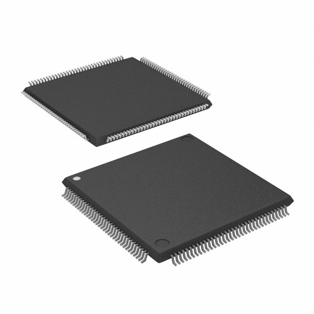
- Package & Mounting — Surface‑mount 100‑pin package (100‑LQFP / supplier package 100‑TQFP 14×14) for PCB space‑efficient integration.
- Industrial Temperature Grade — Rated for operation from –40 °C to +85 °C to meet industrial application environments.
- RoHS Compliant — Device meets RoHS requirements.
Typical Applications
- Industrial Control — Implement motor control logic, timing and interfacing between sensors and controllers where industrial temperature range and robust I/O support are required.
- Embedded Interface Bridging — Provide protocol bridging, glue logic and signal conditioning between 3.3 V and 5 V domains using configurable I/O and 5 V tolerant inputs/drive strength.
- Hot‑Swap & Removable Modules — Use hot‑swap‑capable I/Os and power‑up/power‑down friendly behavior for hot‑swappable cards and modular systems.
- Legacy System Modernization — Replace or augment legacy ASICs and discrete logic in systems requiring deterministic timing and in‑system programmability.
Unique Advantages
- Nonvolatile, Single‑Chip Configuration — Eliminates the need for external configuration memory while simplifying board designs and improving system robustness.
- Mixed‑Voltage I/O Support — Broad supply range and configurable I/O make it straightforward to interface with both 3.3 V and 5 V peripherals, reducing level‑shifter requirements.
- Deterministic Timing — SX‑A family deterministic, user‑controllable timing helps ensure predictable behavior in timing‑sensitive control and interface tasks.
- Security Features — FuseLock™ secure programming technology protects IP and reduces risk of reverse engineering or design theft.
- Industrial Temperature Rating — –40 °C to +85 °C rating supports deployment in factory, field, and other industrial environments.
- Compact Surface‑Mount Package — 100‑pin LQFP/TQFP package enables high‑density PCB designs while providing 81 user I/Os.
Why Choose A54SX08A-1TQ100I?
The A54SX08A-1TQ100I delivers a compact, nonvolatile FPGA option with around 12,000 system gates and 768 logic elements for mid‑range control and interface tasks. Its flexible I/O, wide supply voltage window and industrial temperature rating make it well suited to industrial systems, embedded controllers, and modular hardware that require reliable, in‑system programmability and strong IP protection.
Designers seeking deterministic timing, hot‑swap capability and a single‑chip configuration solution will find the A54SX08A‑1TQ100I aligns with demanding board‑level integration and long‑term deployment needs while simplifying BOM and configuration management.
Request a quote or submit an inquiry to receive pricing, availability and technical support for the A54SX08A-1TQ100I. Our team can assist with ordering and application details to help integrate this FPGA into your design.


Date Founded: 1989
Headquarters: Chandler, Arizona, USA
Employees: 22,000+
Revenue: $8.349 Billion
Certifications and Memberships: ISO9001:2015, IATF16949:2016, AS 9100D


